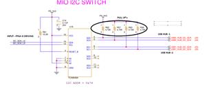
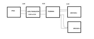
Part Number: TCA9546A
Hi Team,
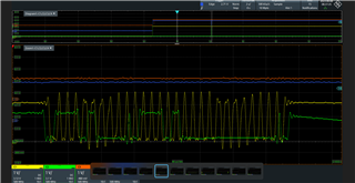
We are using I2C Switch to connect 2 USB HUB (P/N- USB5744).We are facing USB HUB detection issue.At the time of Probe we obsrve that SDA signal level is not raching to 3.3V level.Can you please suggest what can be the issue?
Probe point-
SCL-R57
SDA-R62
Note- Before I2C Switch level SCL and SDA LEVEL ar 3.3V.
SCH
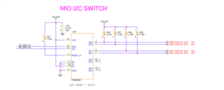
WAVEFORM
Many Thanks
Rajat