Part Number: DS90UB949A-Q1
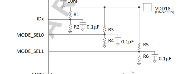
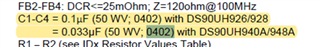
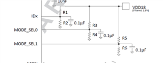
1, 949 C1-C4 note 50WV, 0402, what’s the meaning of 50WV?
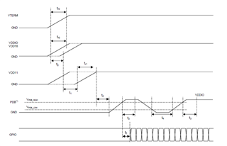
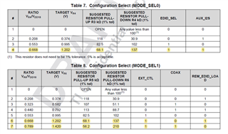
2,configure PIN add 0.1u, when the sampling time? If the up resistor bigger, power up RC will need time.
Part Number: DS90UB949A-Q1
1, 949 C1-C4 note 50WV, 0402, what’s the meaning of 50WV?
2,configure PIN add 0.1u, when the sampling time? If the up resistor bigger, power up RC will need time.