Part Number: XIO1100
Hi,
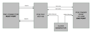
Please find the below attached block diagram, We are going to use FMC Connector as Root port and PCIE finger edge as END POINT, we want to know that the mentioned PCIE PHY PART (XIO1100ZWSR) will support this configuration. If the PCIE PHY supports this configuration, Kindly provide a solution for the clock generator also please suggest the suitable clock part and we are going to use 100MHz differential clock for PCIE PHY and also for Finger edge.