This thread has been locked.

If you have a related question, please click the "Ask a related question" button in the top right corner. The newly created question will be automatically linked to this question.

TMDS181: What information is included in the DDC circuit in addition to the EDID information?

Part Number: TMDS181


Dears:

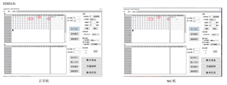
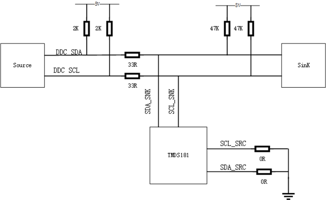
The picture shows two connection modes of DDC circut

Paranormal:The display appears unusually at 4k@60hz resolution,When DDC circuit in accordance with Figure 1;

But the display appears normally at 4k@60hz resolution,When DDC circuit in accordance with Figure 2.

The display appears normal in both connection modes at 4k@30hz resolution.

I want to know:

What causes the discrepancy?

What‘s the reason that the display appears unusually when the normal EDID information is obtained in fig 1?

  • Read the register value is 0XDA accoring to DDC on mode(fig 2),but that is 0XC0 accoring to snoop mode(fig 1). 

    Look at the reference specifications,the TMDS_CLOCK_RATIO_STATUS is incorrect in snoop mode.

    I can't understand what‘s the reason that DDC mode can effect the result of  register value

  • Hello,

    To answer the first questions, the TMDS_CLOCK_RATIO_STATUS needs to be set to 1 for the right HDMI 2.0 TMDS clock and this would certainly cause a problem with the image.

    How are the TMDS181 SDA_SNK, SCL_SNK, SDA_SRC & SCL_SRC pins configured in figure 1?

    Could you also provide the DDC bus traffic data?

    Thanks,

    Zach

  • There is currently an error in the fetch register, but it is not clear what caused it?Line impedance, source problem, or TMDS181 exception?

    But the strange thing is that after changing the DDC mode, the register reads correctly and the exception disappears.This seems to have something to do with TMDS181.

  • Hello,

    There should only be one pair of pull up resistors on the bus.

    I recommend removing the 2k ohm pull up resistors and the 33 ohm resistors on the DDC bus as you are showing above.

    Thanks,

    Zach

  • Hello,

     The 2k ohm pull up resistors are part of the source.Like OPS(windows), is a Microcomputers.I can't change it.

    If removing the 47k ohm pull up resistors and the 33 ohm resistors on the DDC bus,that should be equivalent to your suggestion.

    Thanks

  • Hello,

    Since HDMI 1.4 will display normally, I don't think it has anything to do with the DDC physical path.

    So the TMDS_CLOCK_RATIO_STATUS determines based on what information is on the DDC path and then changes from 0 to 1,when the EDID switches from 1.4 to 2.0?

  • Hello,

    As part of discovery, the source reads the sink’s EDID information to understand the capabilities of the sink and part of this read determines the data rate supported. Depending upon the data rate, the source writes to sink address 0xA8 offset 0x20 bit1, TMDS_CLOCK_RATIO_STATUS. The TMDS181 snoops this write to determine the TMDS clock ratio and thus sets its own TMDS_CLOCK_RATIO_STATUS bit accordingly.

    Thanks,

    Zach