This thread has been locked.

If you have a related question, please click the "Ask a related question" button in the top right corner. The newly created question will be automatically linked to this question.

TCAN4550EVM: CAN initialization failure with STM32F407/Keil compiler

Part Number: TCAN4550EVM
Other Parts Discussed in Thread: TCAN4550, , TCAN4550-Q1

Hello,

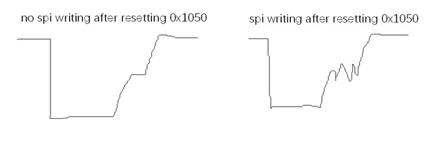
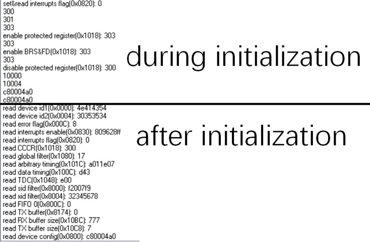
with your help from my last post, I'm able to establish contact with TCAN. Then I tried to 'translate' your code sample to keil code for ST MCU. The initialization was failed. Other CAN devices get no ACK from TCAN. I got a 'Internal Multiple transfer mode access in progress' error immediately after I tried to clear all errors. I recorded the read values from the registers I wrote to in the screenshot. Can you see anything wrong?

What I've done is:

write '0xFFFFFFFF' to 0x000C  (clear ERR flags)

write '0' to 0x0830  (disable interrupts)

read from 0x0820 and write this value back  (clear the interrupt flags)

write '0' to bit 4&3 and '1' to bit 1&0 of 0x1018  (enable protected register)

read from 0x1018, apply mask (~(0xFFFF0C00 | 8)), set '1' to bit 9,8,1,0, and write back  (enable BRS, FD, CCE, INIT)

write '1' to bit 4,2,1,0 of 0x1080  (accept global messages to FIFO0)

write '5<<25 | 1<<16 | 30<<8 | 7' to 0x101C  (SJW=6, prescaler=2, tseg1=31, tseg2=8)

write '0<<16 | 13<<8 | 4<<4 | 3' to 0x100C  (prescaler=1, tseg1=15, tseg2=5, SJW=4)

write '14<<8' to 0x1048  (TDCO=15)

write '0' to memories from 0x8000 to 0x87FF  (clear memories)

write '0' to 0x1084  (standard filter address = 0x8000)

write '4' to 0x1088  (extended filter address = 0x8004)

write '0x800C | 5<<16 | 0x80000000' to 0x10A0  (RX FIFO0 elements =5, address =0x800C)

write '0x8174 | 0<<16 | 0x80000000' to 0x10B0  (RX FIFO1 elements =0, not used)

write '0x8174' to 0x10AC  (RX buffer elements =0 , not used)

write '0x8174 | 0<<16' to 0x10F0  (RX buffer elements =0, not used)

write '0x8174 | 2<<24 ' to 0x10C0  (TX buffer elements =2, address =0x8174)

write '7<<8 | 7<<4 | 7' to 0x10BC  (RX buffer size = 64 bytes)

write '7' to 0x10C8  (TX buffer size = 64 bytes)

write '0' to bit 4,3,1,0 of 0x1018  (disable protected register)

write '1' to 0x1054  (enable RX FIFO0 interrupt on nINT)

write '0<<30 | 1<<27 | 0x720<<16 | 0x7F9' to 0x8000  (standard id filter: SFT=0(range filter), SFT=1(store in FIFO0), SID1=0x720, SID2=0x7F9)

write '1<<29 | 0x12345678' to 0x8004 and '2U<<30 | 0x1FFFFFFF' to 0x8008  (xid filter: EFEC=1, id=0x12345678, EFT=2, mask=0x1FFFFFFF)

write '3U<<30| 1<<27 | 1<<10 | 1<<5' to 0x0800  (device config register)

write '2' to bit 7&6 of 0x0800  (normal mode)

write '0xFFFFFFFF' to 0x1050  (clear all interrupts)

  • Hello Reko,

    write '0' to 0x1084  (standard filter address = 0x8000)

    There will be No Standard ID Filters because LSS[7:0] (bits 23:16) are set to 0's.  I see you are trying to write a single SID filter element, so the register of 0x1084 is incorrect. 

    write '4' to 0x1088  (extended filter address = 0x8004)

    There will be No Extended ID Filters because LSE[6:0] (bits 6:0) are set to 0's.  I see you are trying to write a single SID filter element, so the register of 0x1084 is incorrect.  However, you have set the ANFE field in 0x1080 to accept all non-matching frames, so you should still receive the messages if you don't have a XID filter.

    You have set the ANFS and ANFE fields in 0x1080 to accept all non-matching frames to RX FIFO 1, so you should still receive the messages if you don't have a SID/XID filter element created.  Your notes say you have allocated 0 (or NO) RX FIFO 1 elements, so this may cause problems with accepting your non-matching frames and you should change this to store them in RX FIFO 0 or allocate RX FIFO 1 elements.

    However, I'm having difficulty validating your configuration.  Can you confirm the final hex values you are writing to the configuration registers instead of the logic you are using to write to these registers?  When I try to verify the number of RX FIFO 0/1 and RX/TX Buffer elements, I'm getting different values than what you are describing in your comments.  This could either mean that I am not following your OR and bit shift descriptions to get the final register configuration value and I can't properly review your configuration, or there is a problem with your register configuration.

    If you could please just provide a list of final register values for my review, I could better help validate your configuration.

    Regards,

    Jonathan

  • Hello. Thank you for finding my mistakes. I should connect the global filter to FIFO 0, as your code sample does. In fact I tried to copy most parameters from the sample. But CAN function still doesn't work after correcting it.
    For the filters of SID and XID, I've given the wrong values in the post. In my code I put '<address>|1<<16'. In order to avoid such mistakes, I add more lines to confirm the written and read-back values for each write operation. And I read from all registers again after the initialization is done. The following response are sent from MCU to PC via COM, except the comment I added later. All values are hex.

    //clear all ERR flags
    write to 0x000C: 0xFFFFFFFF
    read from 0x000C: 8 //I got this error "internal access active", don't know the meaning
    //disable interrupts
    write to 0x0830: 0
    read from 0x0830: 809628ff //also problematic, because 809628ff & REG_BITS_DEVICE_IE_MASK = 0x80000000, should be 0
    //clear interrupt flag
    0 //read value is already 0, MCU reports the response by each reading
    write to 0x0820: 0
    read from 0x0820: 0
    //enable protected register
    300
    301
    303 //retry 3 times and succeeded
    write to 0x1018: 303
    read from 0x1018: 303
    //enable BRS&FD, already enabled, just do it again like the code sample, why not combine with the last step
    write to 0x1018: 303
    read from 0x1018: 303
    //set global filter
    write to 0x1080: 3 //reject remote frames, put others to FIFO 0
    read from 0x1080: 3
    //Nominal Bit Timing & Prescaler
    write to 0x101C: A011E07 //SJW=6, prescaler=2, tseg1=31, tseg2=8
    read from 0x101C: a011e07
    //write to Data Bit Timing & Prescaler register
    write to 0x100C: D43 //prescaler=1, tseg1=15, tseg2=5, SJW=4
    read from 0x100C: d43
    //Transmitter Delay Compensation Register
    write to 0x1048: E00 //TDCO = 15
    read from 0x1048: e00
    //SID filter
    write to 0x1084: 10000
    read from 0x1084: 10000
    //XID filter
    write to 0x1088: 10004
    read from 0x1088: 10004
    //RX FIFO 0
    write to 0x10A0: 8005000C //set the number to 5, do I need so many?
    read from 0x10A0: 8005000c
    //RX FIFO 1
    write to 0x10B0: 80000174 //the sample use no RX FIFO1 but still set the memory address
    read from 0x10B0: 80000174
    //RX buffer
    write to 0x10AC: 174 //the sample use no RX buffer but still set the memory address
    read from 0x10AC: 174
    //TX FIFO
    write to 0x10F0: 174 //the sample use no TX FIFO but still set the memory address
    read from 0x10F0: 174
    //TX buffer
    write to 0x10C0: 2000174 //buffer size =2
    read from 0x10C0: 2000174
    //RX buffer
    write to 0x10BC: 777
    read from 0x10BC: 777
    //TX buffer
    write to 0x10C8: 7
    read from 0x10C8: 7
    //disable protected register
    303
    write to 0x1018: 300
    read from 0x1018: 300
    //enable MCAN interrupts
    write to 0x1054: 1
    read from 0x1054: 1
    //extended id filter
    10000 //read the address from 0x1084
    write to 0x8000: F2007F9 //SFT=0(range filter), SFEC=1(store in FIFO0), SID1=0x720, SID2=0x7F9
    read from 0x8000: f2007f9
    //extended id filter
    10004 //read the address from 0x1088
    write to 0x8004: 32345678 //EFEC=1(store in FIFO0), ID=0x12345678
    read from 0x8004: 32345678
    write to 0x8008: 9FFFFFFF //EFT=2(classic filter), mask=0x1FFFFFFF
    read from 0x8008: 9fffffff
    //device configuration register
    c80004a0
    write to 0x0800: C80004A0 //WAKE_CONFIG = bi-direction, CLK_REF = 40MHz, GPIO1 GPO = MCAN INIT1, forced 1 by writing
    read from 0x0800: c80004a0
    //set mode
    c80004a0
    write to 0x0800: C80004A0 //normal mode
    read from 0x0800: c80004a0
    //clear all interrupts
    write to 0x1050: FFFFFFFF
    read from 0x1050: 0
    //read all configurations again
    read device id1 (0x0000): 4e414354
    read device id2 (0x0004): 30353534
    read error flag (0x000C): 8
    read interrupts enable (0x0830): 809628ff
    read interrupts flag (0x0820): 0
    read CCCR (0x1018): 300
    read global filter (0x1080): 3
    read arbitrary timing (0x101C): a011e07
    read data timing (0x100C): d43
    read TDC (0x1048): e00
    read sid filter (0x8000): f2007f9
    read xid filter (0x8004): 32345678
    read FIFO 0 (0x800C): 0
    read TX buffer(0x8174): 0
    read RX buffer size (0x10BC): 777
    read TX buffer size (0x10C8): 7
    read device config (0x0800): c80004a0

    The problem occurs at the very 1st step. The error 'internal access active' has the description 'Internal Multiple transfer mode access in progress'. I don't understand its meaning. Maybe I did something wrong with the wiring? Besides the SPI wires, I only connected the 5V and GND to MCU. I'm not ready to test the interruption so nINT is not connected. Are there other pins I should pay attention to?
    My current code is full of redundancies and may not be helpful, so I didn't upload them. The SPI connection is OK now and feedback should be trustful.

  • Hello Reko,

    Let's walk through your configuration...

    read from 0x000C: 8 //I got this error "internal access active", don't know the meaning

    The internal access active is not an error, it is just a status indication stating that the device is accessing internal memory locations such as registers or MRAM memory cells.  Not all status bits are errors.  It is normal to see this internal access active bit set.

    //disable interrupts
    write to 0x0830: 0
    read from 0x0830: 809628ff //also problematic, because 809628ff & REG_BITS_DEVICE_IE_MASK = 0x80000000, should be 0

    All of the bits that are set to 1 in your read from 0x0830 is a read only reserved bit that has a default value of 1, so you likely will not read back 0x00000000 after writing 0x00000000 to this register.

    //enable protected register
    300
    301
    303 //retry 3 times and succeeded

    Writing to this register multiple times is expected.  The first write sets the INIT bit.  Then the second write allows the CCE bit to be set.  Then once these two bits are set, the other "protected" bits in this register can be set, so 3 times is expected the first time.  You could leave the CCE bit set and then just change the INIT bit for future protection and reduce future write cycles to 2 writes, but generally INIT and CCE are set together and there is a total of 3 writes.

    //Nominal Bit Timing & Prescaler
    write to 0x101C: A011E07 //SJW=6, prescaler=2, tseg1=31, tseg2=8
    read from 0x101C: a011e07

    This should set your Nominal bit time to 500kbps with an 80% sample point. 

    //write to Data Bit Timing & Prescaler register
    write to 0x100C: D43 //prescaler=1, tseg1=15, tseg2=5, SJW=4
    read from 0x100C: d43

    This should set your Data bit time to 2Mbps with an 80% sample point.  However, for CAN FD with faster bit rate switching during the data phase, you will need to enable the Transmitter Delay Compensation (TDC) bit 23 to 1.

    //Transmitter Delay Compensation Register
    write to 0x1048: E00 //TDCO = 15
    read from 0x1048: e00

    Typically the TDCO value is set to the equal to the number of tq before the sample point in the Data bit field.  This field is not interpreted as 1 greater than the value because 0 is a valid number.  Therefore, since you have 15 tq in the bit period before the sample point, you would set TDCO to 0xF (decimal 15).  The total register value would be 0x00000F00.  It may work with a value of 0xE and this would possibly result in an internal Secondary Sample Point (SSP) used during the transmission phase of 75% instead of 80%. 

    //SID filter
    write to 0x1084: 10000
    read from 0x1084: 10000

    This will enable 1 SID filter element with a start address of 0x8000 in the MRAM space.  Each SID filter element occupies 4-bytes or 1-word of memory.

    //XID filter
    write to 0x1088: 10004
    read from 0x1088: 10004

    This will enable 1 XID filter element with a start address of 0x8004 in the MRAM space.  Each XID filter element occupies 8-bytes or 2-words of memory.  This looks correct because it allows for 1 word of memory needed for the SID filter.

    //RX FIFO 0
    write to 0x10A0: 8005000C //set the number to 5, do I need so many?
    read from 0x10A0: 8005000c

    This will enable 5 RX FIFO 0 elements with a start address of 0x800C in the MRAM space.  This looks correct because it allows for 2 words of memory needed for the XID filter.  The amount of RX FIFO elements needed would depend on how many unread messages you need to hold in the time between the MCU checking for new messages.  It doesn't hurt to have unused RX FIFO elements, but if you don't have enough you may lose messages if the FIFO becomes full.

    //RX FIFO 1
    write to 0x10B0: 80000174 //the sample use no RX FIFO1 but still set the memory address
    read from 0x10B0: 80000174

    This will not enable any RX FIFO 1 elements because the F1S[6:0] is set to 0x0.  Therefore the MRAM Start Address will be ignored.  You could set the start address to any value you would like as long as the number of elements is set to 0.

    //RX buffer
    write to 0x10AC: 174 //the sample use no RX buffer but still set the memory address
    read from 0x10AC: 174

    The RX Buffers are not given a specific count like the RX FIFOs.  You must keep track of how many RX Buffers you have allocated through the number of data bytes you assign for RX Buffers through the RBDS[2:0] field of register 0x10BC and the start addresses used in your configuration.  The only way to receive a message into a dedicated RX Buffer element is through a Filter element.  Therefore, you will need to determine how many dedicated RX Buffer elements you will need based on your filters, and then then calculate the start address and end address in your MRAM configuration so that you don't have overlapping memory allocations.  If you don't plan on using the dedicated RX Buffers then your start address shouldn't matter.

    //TX FIFO
    write to 0x10F0: 174 //the sample use no TX FIFO but still set the memory address
    read from 0x10F0: 174

    This is the TX Event FIFO, not the TX Transmit FIFO.  This FIFO holds records of successful transmission events for the MCU to monitor if desired.  But if the Event FIFO Size bit field is set to 0, the start address is ignored.

    //TX buffer
    write to 0x10C0: 2000174 //buffer size =2
    read from 0x10C0: 2000174

    This will enable 2 TX Buffer elements in a TX FIFO configuration with a start address of 0x8174 in the MRAM space.  Because the previous elements have been unused, this start address looks correct and allocates the correct number of words needed for the RX FIFO 0 (90 words).

    //RX buffer
    write to 0x10BC: 777
    read from 0x10BC: 777

    You have set the data field size to 64 bytes for all types of RX buffer and FIFO elements even though you are only using the RX FIFO 0 for messages.  This is OK and the field associated with the unused element types doesn't matter.

    //TX buffer
    write to 0x10C8: 7
    read from 0x10C8: 7

    You have set the data field size to 64 bytes for the TX buffer/FIFO elements.

    //disable protected register
    303
    write to 0x1018: 300
    read from 0x1018: 300

    This should write protect the configuration registers.

    //enable MCAN interrupts
    write to 0x1054: 1
    read from 0x1054: 1

    This will enable the RX FIFO 0 new message interrupt to be reflected on the interrupt line.

    10000 //read the address from 0x1084
    write to 0x8000: F2007F9 //SFT=0(range filter), SFEC=1(store in FIFO0), SID1=0x720, SID2=0x7F9
    read from 0x8000: f2007f9

    This element is configured correctly based on your comments.

    //extended id filter
    10004 //read the address from 0x1088
    write to 0x8004: 32345678 //EFEC=1(store in FIFO0), ID=0x12345678
    read from 0x8004: 32345678
    write to 0x8008: 9FFFFFFF //EFT=2(classic filter), mask=0x1FFFFFFF
    read from 0x8008: 9fffffff

    This element is configured correctly based on your comments.

    //device configuration register
    c80004a0
    write to 0x0800: C80004A0 //WAKE_CONFIG = bi-direction, CLK_REF = 40MHz, GPIO1 GPO = MCAN INIT1, forced 1 by writing
    read from 0x0800: c80004a0
    //set mode
    c80004a0
    write to 0x0800: C80004A0 //normal mode
    read from 0x0800: c80004a0

    This will set the device to Normal mode and the configuration looks correct based on your comments.

    Everything looks generally OK to me with maybe a slight change to the TDCO value. 

    Are you still unable to communicate with these settings? Are you reading the status and interrupt registers after you try to send a message to the TCAN4550?  Are any new bits set that are different from your initial values that you read during your configuration sequence?

    Are you able to monitor the CANH and CANL lines for activity when you try to transmit or receive a message?  You can also monitor the Error Counter Register (0x1040) and the Protocol Status Register (0x1044) if you think you are getting CAN bus activity, but the messages contain errors. 

    Have you tried to transmit a message?  If so, what is the message content and to which MRAM address are you writing that to? With a TX FIFO configuration that has 2 elements, you will need to keep up with the correct buffer to use for the messages through the TX FIFO/Queue Status register (0x10C4).  But you should be able to receive messages sent from another device on the bus.

    Regards,

    Jonathan

  • Thank you very much for going through every setup step for me. It turns out the problem lies in the CAN cabled which was already connected when TCAN4550EVM was handled to me from the other colleague. Since I have lots of questions about the coding, it didn't become my suspect until you verified my configuration. Now I have succeeded in acknowledge received messages and send mine.

    As for the data bit rate setting, I intended to set the sample point to 75% as the code sample does. I made a mistake in my comment. TSeg1 I have used is 14 instead of 15. 'DataTqBeforeSamplePoint' used by the sample is 15(tseg1 + 1 synchronous bit). And the written value is 15-2 according to the comment in the code sample.

    The 2nd step is still a little confusing to me though you said my response is normal. From what I understand from the code sample, 0 is written to TCAN and a return value(ANDed by the MASK) should be equal to the written value. Mine is 1 bit different. 

    bool
    TCAN4x5x_Device_ConfigureInterruptEnable(TCAN4x5x_Device_Interrupt_Enable *ie)
    {
        AHB_WRITE_32(REG_DEV_IE, ie->word);
    #ifdef TCAN4x5x_DEVICE_VERIFY_CONFIGURATION_WRITES
        // Check to see if the write was successful.
        uint32_t readValue = AHB_READ_32(REG_DEV_IE);       // Read value
        readValue &= REG_BITS_DEVICE_IE_MASK;               // Apply mask to ignore reserved
        if (readValue != (ie->word & REG_BITS_DEVICE_IE_MASK))
            return false;
    #endif
        return true;
    }

    And I have saved the question about FIFOs and buffers until my major problem is solved now. The code sample uses only FIFO 0 for RX and buffer for TX. RX buffer and TX FIFO are disabled. What's the difference between using FIFO and buffer? RX FIFOs and buffer are distributed by filters, but what about TX? Will all sent messages go through the buffer first and then TX FIFO?

  • Hi Reko,

    I'm glad to hear your setup is communicating.

    I'm sorry for misunderstanding your second step question.  I overlooked the AND'd value portion of it and that you were specifically questioning why bit 31 is set to '1' instead of '0' after the AND. 

    //disable interrupts
    write to 0x0830: 0
    read from 0x0830: 809628ff //also problematic, because 809628ff & REG_BITS_DEVICE_IE_MASK = 0x80000000, should be 0

    Do I now have the correct understanding of your question?

    If so, you may be working with an older version of the demo code that had an incorrect mask value and bit 31 was incorrect.  This was updated in version 1.2.2 on 6/8/2020.

     *  Updated 6/8/2020
     *      - 1.2.2: Corrected incorrect mask value for REG_BITS_DEVICE_IE_MASK (bit 31 is now 0)
     
     
     //The corrected mask was changed to the following value in this code:
     #define REG_BITS_DEVICE_IE_MASK                     0x7F69D700 //! This mask is the bitwise-inverse of the 0x0830 IE register's reserved bits. A reserved bit is read as high always. This masks the reserved bits out.

    And I have saved the question about FIFOs and buffers until my major problem is solved now. The code sample uses only FIFO 0 for RX and buffer for TX. RX buffer and TX FIFO are disabled. What's the difference between using FIFO and buffer? RX FIFOs and buffer are distributed by filters, but what about TX? Will all sent messages go through the buffer first and then TX FIFO?

    You can use a combination of RX FIFO and Buffer elements, or only one type based on how you want to structure your application. RX buffers are useful if you have a specific message or messages that can be filtered into a known location that the MCU can retrieve because the address is always fixed.  Different types of messages can have different dedicated buffers and you can manage the messages in this manner.

    However if you receive other messages, or simply want to process them in the order that they were received, the FIFO approach may be more useful.  There are also two different FIFOs that can allow you to still have some separation for different types of messages.

    As I mentioned, you can have both RX FIFO 0, RX FIFO 1, and dedicated RX Buffer elements configured and then use your Filter elements to direct the messages to the various locations based on your application needs.

    The same goes for the TX FIFO or Queue and dedicated buffer elements.  If the MCU needs to only send a few messages infrequently, then dedicated TX Buffers may be the easiest method because the MCU can simply write the message to the buffer location and then set the corresponding bit in the TX Buffer Add Request register to send the message.  These same TX buffer elements can be reused for future messages as long as they have successfully transmitted the previous message.  The MCU can monitor this by reading the TX Buffer Request Pending register.

    There is also a TX FIFO or Queue that can be used as well.  You can't use a FIFO and a Queue at the same time, but you can still have dedicated TX Buffers with either the FIFO or Queue. 

    The TX FIFO will send the messages in the order they are placed into the FIFO, regardless of the message ID.  The Queue differs from the FIFO by first evaluating the message ID's and then prioritizing the transmission based on the lowest message ID value because it has the highest priority per the CAN arbitration protocol and therefore it is assumed this message should be prioritized for transmission in the device.

    The TX FIFO/Queue and dedicated Buffers all use the same 32 TX Buffer elements in terms of the buffer numbers, but they can be allocated to both types allowing you to customize your application.

    The TCAN4550-Q1 uses the MCAN CAN FD Controller IP developed by Bosch, and the MCAN Users Manual should be considered as a supplement document to the TCAN4550-Q1 datasheet because not all of the MCAN information could be included in the datasheet.  The MCAN related registers in the TCAN4550-Q1 have been given an offset of 0x1000, otherwise nothing was changed in the IP itself.  For example, the Control Register in the MCAN Users Manual has an address of 0x18, but it is 0x1018 in the TCAN4550-Q1 device.  This document explains many of the CAN configuration settings in more detail and my be of great benefit to your software development.

    Regards,

    Jonathan

  • Thank you for the detailed explanation. It helps me get a better understanding to the coding work.

    I found only one code sample on the website(the new one has the same file name so I didn't discover the update). Are there other samples which can help me learn to use interrupt and TX FIFO?

  • Hi Reko,

    There is only the one version of the demo code so unfortunately I can't point you to reference for additional examples that use the TX FIFO mode.

    Generally speaking for a FIFO, the MCU will need to monitor the FIFO status register to check the fill level, and Put address to determine which TX Buffer element to place the next message that should be transmitted.

    Regards,

    Jonathan

  • It's OK that no more code samples are available. I just want them to make my learning easier. It's hard to figure out how to set the registers, because some bits accept the value written to them, some are reset by writing 1 to them and some are not to be modified.

    Currently I'm more interested in receiving messages by ISR. The example uses polling and disables all interrupts.

  • Hi Reko,

    Understood.  If there are any specific issues that you just can't figure out, you can always reach out through this forum for support.

    Regards,

    Jonathan

  • ISR still doesn't work for me.

    I find that the example has already enabled the interrupt for RX FIFO 0 (0x1054 set to 1). The other interrupt enabling register 0x0830 is totally 0 but I don't see anything connected to message receiving. So I believe the interrupt is already enabled though only polling is used for message reception. However, I detect no voltage drop (from 3.3V) at nINT during an incoming message via multimeter. Have I missed some operation?

    The configuration parameters are kept the same as above. I'm able to receive messages with codes inside the while loop of the main function. By testing ISR, I moved them away in case they cleared the interrupt as soon as it occurred.

  • Hello Reko,

    What is the value of register 0x105C?  You will likely need to set the Enable Interrupt Line 0 (EINT0) bit 0 to "1".

    The TCAN4550 has a single "Global" interrupt pin (nINT), but the MCAN IP has two Interrupt Lines in the core that can be used to separate the interrupt bits based on priority or type.  Each MCAN interrupt bit can be individually enabled and also assigned to either of the two MCAN Interrupt lines.  This is done through registers 0x1054 and 0x1058.

    The two MCAN interrupt enable lines can then be enabled or disabled through register 0x105C, and by default they are both disabled.  (I don't know why...)

    The nINT pin will represent all enabled and non-masked interrupt bits, but you can also configure the GPO2 and GPIO1 pins to be MCAN Interrupt pins if you want a separate MCAN interrupt pin that won't also contain other types of bits related to voltage, temperature, SPI error, watchdog, etc. 

    For example, some users prefer to have a dedicated interrupt for RX Messages that they can prioritize with the MCU ISR.

    Regards,

    Jonathan

  • You are right! Setting 0x105C enables the interrupts. And it's nice to have separate interrupts. I decided to use GPO2.

    I'm just a little confused about register 0x0824 and 0x1050. They have the same register map, and I only need to care 0x1050. What's the meaning of the former?

  • Hi Reko,

    The registers that have an address of 0x1000 to 0x10FF are part of the MCAN controller IP.  Register 0x1050 is the interrupt register for the MCAN related bit fields.

    The registers that have an address of 0x0800 to 0x08FF are added by TI for device functionality that is not related to MCAN.  Register 0x0820 is the interrupt register for non-MCAN related bit fields.

    In order for the MCU to read all device registers, it would need to read both registers 0x0820 and 0x1050 which requires two separate SPI Read transactions.

    In order to improve SPI efficiency, a Read only copy of register 0x1050 was created with address 0x0824 which is adjacent to register 0x0820.  This allows a single SPI Read transaction to read all interrupts by setting the Length field to "2".  This reduces the overall amount of time needed by the MCU to read the interrupt bits and improves efficiency.

    Regards,

    Jonathan

  • Hello, I've got new problems with receiving messages. I'm not sure which is the better way, to continue asking questions here or to open a new topic.

    The example counts the interrupt times and solves them in the main function. Only RX FIFO0 is used. I used both FIFO 0&1. So I tried to simplify the work and do all the things inside the ISR. The LED of nINT & GPO blink while working properly, but they may stay ON forever after running for some time(not constant). I suppose it's caused by my way of resetting the interrupts.

    I used GPO2 as MCAN interrupt and input it to my MCU. An input pin at MCU set the ISR when GPO2 changes to active. I reset the MCU interrupt at the beginning of the ISR and reset the interrupts on TCAN(write to 0x1050) after dealing with ALL the interrupts. Even if new messages come while old ones are being processed, the final status is inactive so the next new message will trigger the ISR. I don't understand why the interrupts on TCAN can stuck in active status. Are there misunderstandings?

    I tried to read the error status and the read value from 0x0820 is 0x88, only CAN wake up and global error. And an interesting phenomenon is that the read values from the RX FIFO are wrong when the error occurs. Only specific IDs are allowed to my FIFO 0 but another ID(0x211 in my case) is read and calculated out. Other data are not expected as well.

    Do you have any experience in dealing with such issues?

  • Hi Reko,

    The problem with handling everything in the ISR is that it increases the chances for new events to occur while you are handling one interrupt event and hold the interrupt pin low as you are observing.  This means your MCU will essentially stay "stuck" in the ISR and not be able to handle any of the Main Loop functions.  This is why the demo code does as little as possible inside the ISR itself so that the MCU doesn't get stuck.

    If you read the interrupt registers to determine which bits are set, and then don't clear them right away, then the other bits may bet set before the MCU clears the bits, which the MCU didn't realize were set.  So you will need to re-read the interrupt registers a final time at the end of the ISR to determine if there are any new bits that need to be cleared before exiting the ISR.

    Do you know what interrupts are still set, and have you compared the register read values at the beginning of the ISR and at the end?  If all the interrupt bits are cleared, then interrupt pins should get pulled high again.  If it stays low, there are still bits set.

    If you are reading a value of 0x88 from register 0x0820, then you are getting some type of SPI error (bit 3) and the global error (bit 7) is set because the SPI error bit is set.  This can either come from a protocol error with your SPI driver, a signal integrity error causing too many or too few SPI clock cycles/bits to be detected, or from a clock related issue preventing the data coming from the digital core registers or MRAM to pass through the SPI FIFO that handles the system clock to SPI clock frequency domain crossing.

    Do you get this 0x88 value consistently?  If so, we need to figure this issue out because it will keep holding your nINT pin low as well.

    I can look over message filters for configuration errors to see if I can figure out why messages are getting though that you don't think should if you send me the filter information you are writing to your MRAM. 

    Regards,

    Jonathan

  • Hi Jonathan,
    I do understand the risk of doing everything in ISR you are talking about. I did so to control the priorities of different actions and left only unimportant codes in the main loop. And after I went through the demo code again, I found potential risks as well if I understood it correctly.
    The ISR increase the counter when a new message is received, but it doesn't reset the interrupt(by writing to 0x1050) on TCAN immediately. So the counter won't increase until the main loop handles the last message. And it handles only one message with one counter. The received messages can be counted correctly if new messages are received before the interrupt is reset on TCAN.
    This is the problem I've met. At first I copied this strategy though I didn't use the counter and did the things in the ISR. Then I found the message reception became one or more messages slower than the other CAN device in the same network, because ISR got triggered only once when more than one message came into TCAN.
    Then I added a while loop to deal with all the messaged read out from RX FIFOs. But this method also has a serious problem. I cannot guarantee that the interrupts cleared is equal to the messages being dealt with. If I clear the interrupts with the value from 0x1050, the MCU may process more messages(?I'm not sure about this) from RX FIFOs if they come in later. So I tried to use '0xFFFFFFFF'(not sure if it's valid) to clear all interrupts in 0x1050 after processing the messages. This may leave unprocessed messages in RX FIFOs, but at least one position(the one I've just processed) is available. And the next message will cause the MCU to handle all the remaining messages in RX FIFOs.

    Please point out my mistake if I misunderstand the working principles. If this strategy meets a problem, it shouldn't be the one I have now. I mean TCAN's interrupt pins stay active without triggering the ISR of MCU.
    The problem is not very frequently. In fact its probability is quite low. Everything seemed OK until I connected test samples which send cyclic messages to it. The bus load is about 5.5%. It can take quite some time to reproduce the error if I don't send more messages manually.


    Edit: I increased the FIFO buffer and used both FIFO 0&1, which is another reason I don't use the interrupt counter method like the demo code. I don't know how many should I decrease the counter if one message from each FIFO is dealt with. About the message filter, there is also something strange. I didn't set any 'high priority messages' in the filters but I remember seeing it from 0x1050. And I saw in the mcan user manual you gave me that 'the FIFO’s Acknowledge Index should not be written' 'when reading a High Priority Message'. It may be the cause of my problem.
    read device id1 (0x0000): 4E414354
    read device id2 (0x0004): 30353534
    read error flag (0x000C): 8
    read CCCR (0x1018): 300
    read global filter (0x1080): 17
    read arbitrary timing (0x101C): A011E07
    read data timing (0x100C): D43
    read TDC (0x1048): E00
    read sid filter (0x8000): FF107F9
    read xid filter (0x8004): 52345678
    read FIFO 0 (0x800C): 0
    read FIFO 1 (0x8174): 58DC2C6(the sample is receiving messages during the reading)
    read TX buffer (0x82DC): 0
    read RX buffer size (0x10BC): 777
    read TX buffer size (0x10C8): 7
    read TX buffer address (0x10C0): 20002E8
    read interrupt flag (0x0820): 0
    read device config (0x0800): C84004A0
    read interrupt enable (0x0830): 809628FF
    read interrupt register (0x1050): 0
    read interrupt enable (0x1054): 11
    read interrupt line select (0x1058): 0
    read interrupt line enable (0x105C): 3

    Edit2: After another day's trying, I suspect the problem is related to the way I used GPO2. I used to think it was a 3.3V output. Later I found the oscilloscope only showed normal result only when GPO2 was connected to MCU. A multimeter detects no stable voltage on it alone. And each interrupt on GPO2 triggers the ISR twice. 

  • Hi Reko,

    The demo code is simply a starter reference intended to help people get started working with the device and it is not intended to be a gold standard reference for actual application code.  So it is good that you are thinking about and working through these types of scenarios.

    The RX FIFO Get Index, Put Index, and Fill Level values should always be what is used to determine how many messages are processed and from which FIFO elements should be processed first.  The Interrupt bit is simply to alert the MCU that there are one or more messages that need to be processed.

    I think conceptually that once a RX FIFO New Message interrupt bit is set, the MCU should read the RX FIFO Status register to determine the Fill Level and the Get Index which would allow it to calculate which RX FIFO element, or elements, contain messages that need to be read.

    Once it does this, it should be ok to clear the interrupt bit and proceed to read and acknowledge the messages in the RX FIFO.  Any new messages received while these messages are processed will again set the new message interrupt bit indicating that even more messages have arrived.

    However, I think I understand your basic point in that there are a couple of potential scenarios that need to be handled in the way the code is structured.

    One scenario is that new messages arrive changing the Fill Level after the RX FIFO Status register is read, but before the messages from the previous read have been cleared.  If the interrupt bit has already been cleared, the ISR would cause the device to re-read the status register and it would see the same Get index, but a higher Fill Level.  If however, the interrupt bit had not yet been cleared, the new messages would be stored in the RX FIFO but the MCU would not know that new messages have arrived.

    In this situation the MCU should keep track of the how many messages it has in the Fill Level, and how many it has acknowledged which will increase the Get Index.  If the Fill Level increases with a new RX message before it has time to clear an old one, the MCU may be able to detect this by some sort of internal counter that keeps track of increase or decrease of the Fill Level relative to the Get Index. 

    If however, the interrupt bit had not yet been cleared, the new messages would be stored in the RX FIFO but the MCU would not know that new messages have arrived.

    You can either re-read the RX FIFO Status register at the end of clearing all the messages that the MCU thinks are in the element to ensure the Fill Level is set to zero.  If so, it should repeat the RX Read and Acknowledge loop until the RX FIFO is empty.

    Comparing the Get Index and Put Index are also a possible message to determine if the FIFO has been completely cleared.

    Whichever approach you take, I think verifying the RX FIFO Status shows the FIFO is empty at the end of your message reception and processing routine should always allow you to know if new messages have arrived while you were processing existing messages.

    The GPO2 pin is an open-drain pin when it is used as an interrupt, so it requires a pullup resistor to VIO (typically 3.3V).  When the device is used in Test Mode it becomes a driven digital output type to mux out either the MCAN TXD signal, or the transceiver's RXD signal.

    Regards,

    Jonathan

  • Hi Jonathan, thank you for the detailed analysis. It helps me understanding about the working principle.

    At first, I nearly excluded the hardware issue. GPO2 was connected to a GPIO which is already pulled up to 3.3V. And 5V and GND of TCAN are connected to those of the MCU board. It's a little weird that the voltage is about 0.02V lower at the MCU side on both 3.3V and GND. Maybe as a result, resetting TCAN interrupts through writing to 0x1050 triggers the ISR the second time if followed by another SPI write action. The oscilloscope shows a small vibration in the uprising curve. This doesn't happen if I hold 10ms after 0x1050 is written to. But I don't think it's the main cause of my current problem.

    I tried several interrupt resetting strategies inside the ISR:

    1. reset interrupt on MCU -> reset 0x1050(by the value read out or 0xFFFFFFFF) -> loop until the fill level is 0 in RX 0 -> loop until the fill level is 0 in RX 1

    2. reset interrupt on MCU -> loop until the fill level is 0 in RX 0 -> loop until the fill level is 0 in RX 1 -> reset 0x1050(by the value read out or 0xFFFFFFFF)

    3. loop until the fill level is 0 in RX 0 -> loop until the fill level is 0 in RX 1 -> reset 0x1050(by the value read out or 0xFFFFFFFF) -> reset interrupt on MCU

    None can avoid the issue that TCAN has the interrupt ACTIVE without triggering the ISR, which means the reception ISR is stuck forever.

    I assigned UDS messages to RX0 and common ones to RX1. Common messages are frequent. UDS messages are sent manually but consumes more processing time. The issue happens mostly by incoming UDS messages. Common messages are in large number so I added lines to monitor the processing of RX FIFO0 only. Through the information I got, the last processing of UDS message is successful and the value of 0x10A4 is 0(fill level). Then the problem happens. I read the values again and its value becomes 0x01010105. The value in 0x1050 is 0x955.

    Do you have any suggestion about the possibility that GPO2 and nINT can become active without triggering MCU ISR?

  • Hi Reko,

    I'm not sure I completely follow you with regards to the GPIO voltage levels.  I believe you are using the TCAN4550EVM which has an adjustable LDO that supplies the VIO voltage to the TCAN4550-Q1.  The VIO voltage sets the Digital IO signal levels and supplies the crystal oscillator circuit.  You should set the VIO voltage to match the MCU levels.  You can find the board's schematic in the TCAN4x5x Evaluation Module User's Guide.  There are no voltage polarity protection diodes on the 3.3V and 5V supply rails, so I don't know why there is a 0.2V voltage drop at the MCU side.  Also note, that if the S4 dip switch is closed for the GPO2 pin to enable the LED, then there is a 10k pullup resistor to the EVM's VIO rail connected to GPO2.  If the dip switch is open, this pullup resistor is removed from the GPO2 net.

    One of the advantages of the TCAN4550 is the SPI interface which allows the device to add a CAN channel to MCU's that either don't have a CAN controller, or as an additional CAN channel if there are not enough CAN controllers available in the MCU.  However, this SPI interface does place some limitations on the overall message frequency that can be achieved due to the extra time required to communicate through the SPI interface.

    I don't know how fast your messages are being transmitted to the TCAN4550, but is sounds like they are coming faster than you are able to process them which is resulting in full FIFOs and perpetual interrupts.

    Can you try an experiment by slowing down the CAN message frequency to see if the interrupts get cleared as you expect as long as new messages are not arriving fast enough to fill the FIFOs?

    The nINT pin is the Logical OR of registers 0x0820 and 0x0824 that have not had the bits masked.  Register 0x0830 is the Enable Mask register for the bits in register 0x0820 and you can disable any of the interrupt bits you don't care about causing a state change on the nINT pin.  This is a Global Interrupt pin and will reflect any and all enabled device interrupt bits.

    Register 0x0824 is a read only copy of register 0x1050 and register 0x1054 is the Enable Mask for these registers that you can use to disable any bits you don't care about.

    The nINT pin will be set as long as any enabled bit in either of these registers has been set to "1" and you can read these registers to determine which bits are holding the nINT pin in an active state.

    With regards to the MCAN interrupts, note that the MCAN controller has two Interrupt lines that can be used to pass separate the interrupts allowing you to isolate some of the interrupts to another pin such as GPO2 or GPIO1 (if configured to be used as such through register 0x0800).

    The Interrupt Line Select register 0x1058 allows you to select which Interrupt line (0 or 1)  is used for that particular interrupt signal.  Register 0x105C allows you to enable or disable these Interrupt Lines. 

    Because GPO2 and GPIO1 are only used for MCAN specific interrupts, they will stay set whenever an interrupt bit that is assigned to that line is set.  This means that these pins may have a different pin state than the global nINT pin, and may be a better option for an ISR routine for CAN messages instead of using the global nINT pin that could be set for any reason.

    How do you have your VIO voltage and Interrupts configured?

    Regards,

    Jonathan

  • You are right. TCAN4550-Q1 is the module I'm using. It's quite convenient and reliable. Once I burned a voltage supply wire on it but it still works normally after the accident.

    The LEDs of GPO2 and nINT are enabled by default. I measure the voltage on GPO2 again and it's 3.3V. It seems that I made a mistake in my last measurement.

    The message frequency is far from the communication capability of TCAN I believe. Perhaps my improper explanation caused your misunderstanding. The value in 0x1050 becomes 0x955 after the ISR missed the voltage drop signal of GPO2 and can never be triggered again. The messages are not processed for some time so the fill level becomes full. When working normally, TCAN is fast enough to suppress the fill level to 1. By the way, the network I'm using is 500k/2M and the bus load is only 5%.

    I assigned RX FIFO 0&1 to mcan_int0 and set GPO2 as mcan_int0. So both RXs can trigger the interrupt on GPO2.

    I added some command to give feedback at the critical points of the ISR. I see the last procedure of the ISR ends properly with writing 0xFFFFFFFF to 0x1050. And the fill level and put/get index seem to be the right value as well.

    ...

    0x1050:10
    0x10B4:20101(fill level=1, process the message)
    0x10B4:20200(fill level=0, break out of the loop)
    reset1050


    0x1050:10
    0x10B4:30201(fill level=1, process the message)
    0x10B4:30300(fill level=0, break out of the loop)
    reset1050

    The next ISR never comes.

    The external interrupt at MCU side is reset at the beginning of the ISR so it's ready to be triggered again long before 0x1050 resets TCAN. The only reasons I can think of is that either the interrupt of MCU is not reset or the command written to 0x1050 doesn't reset TCAN. Do you think the second assumption is possible? For example, a new message comes right at the time TCAN gets the command and has started pulling down the voltage.

    If this problem cannot be solved directly, maybe I should find another way to get around, such as cyclically examining the voltage level on GPO2 and the status of ISR.

    The other problem with even lower possibility is the one I mentioned once. I set 4 filters with IDs assigned to RX FIFO0. The others are assigned to RX FIFO1 by the global filter. When this error happens, messages of an ID which should go to RX1 are processed by the codes for RX0. 

    ......

    0x1050:10 (new message in RX1)
    0x10B4:20101 (0x10B4 is read means it's in the loop for RX1, this is normal)
    0x10B4:30201
    0x10B4:30300 (fill level=0, break out of the loop)
    reset1050


    0x1050:101 (new message in RX0 and 'Timestamp Wraparound', what does it mean?)
    0x10A4:401 (0x10A4 is read means it's in the loop for RX0)
    8A 101,4,211 (the last number is the hex value of the message id=0x211, it should go to RX1 instead)
    0x10A4:0 (fill level=0, break out of the loop)
    reset1050


    0x1050:10
    0x10B4:302
    0x10B4:401
    0x10B4:0

    ......(jump to 100ms later which is the cycle of id=0x211)
    0x1050:10
    0x10B4:40301
    0x10B4:401
    0x10B4:0
    reset1050


    0x1050:101 ('Timestamp Wraparound' again, does it suggest the cause of this error?)
    0x10A4:10001 (when next abnormal loop shows a pattern that the 'get/put index' is weirdly continuous from RX1->RX0->RX1, 4->0->1)
    8A 101,0,211 (get index =0, id=211)
    0x10A4:10100 (fill level=0, break out of the loop)
    reset1050


    0x1050:10
    0x10B4:20002
    0x10B4:20101
    0x10B4:20200

    reset1050

    ......

    There are normal messages of other IDs active but only id=0x211 is taken into RX0 every time the error occurs. I haven't prepared codes to read the filters so I couldn't confirm the condition of the filters. I plan to reproduce this issue after the first problem is solved. Do you know in what condition it may happen?

  • Hi Reko,

    Thank you for the clarification.  There are many factors that contribute to what the maximum bus load that can be supported, but unless the SPI bit rate or processor is very slow, you should easily be able to support 5%.  Getting the data into and out of the TCAN4550 through the SPI bus is the limiting factor to ensure the RX/TX buffer elements don't fill up.

    The external interrupt at MCU side is reset at the beginning of the ISR so it's ready to be triggered again long before 0x1050 resets TCAN. The only reasons I can think of is that either the interrupt of MCU is not reset or the command written to 0x1050 doesn't reset TCAN. Do you think the second assumption is possible? For example, a new message comes right at the time TCAN gets the command and has started pulling down the voltage.

    If this problem cannot be solved directly, maybe I should find another way to get around, such as cyclically examining the voltage level on GPO2 and the status of ISR.

    Is there a way to poll register 0x1050 immediately after you have cleared it with 0xFFFFFFFF to see what the new value is and to determine whether any new bits are set, or remain set?

    If possible, can you try to monitor or the actual GPO2 pin voltage during this process so we can see how it is responding to the read/write sequence of register 0x1050 using a logic analyzer or scope connected to the SPI and GPO2 signals?

    Using the MCU to read the GPO2 pin voltage as high or low could also work as you suggested to see if it is low immediately following a write of 0xFFFFFFFF to register 0x1050 which we know should clear all interrupts and pull GPO2 pin high.  If it is low, then this would indicate it is not safe to exit the ISR.

    Hopefully we can figure out why the MCU is not seeing the GPO2 or why it is staying low with some more direct observational data.  But in the meantime, here are some other ideas for thought.

    It might be interesting to try to use the RX FIFO Watermark interrupt bits on the other MCAN interrupt line brought out on GPIO1.  If the GPO2 interrupt should trigger on every new RX message, then in theory the FIFO watermark level should not be reached assuming the RX FIFO is large enough to have a high watermark level that is beyond what the MCU should allow to be reached.  Then if the only interrupt bit set for the GPIO1 line is the watermark level, it should only get triggered if the MCU fails to act on the GPO2 interrupt pin if it is getting stuck low.

    You could also try to set up some type of timer that would cause the MCU to poll for new messages if it has not received an interrupt from GPO2 within a specified time, sort of like a watchdog.  Then every time the GPO2 triggers the ISR, this timer could be reset which would give you a method of recovery if the GPO2 line gets stuck.

    0x1050:101 (new message in RX0 and 'Timestamp Wraparound', what does it mean?)

    There is an internal counter that is used to create a timestamp that can be used for tracking and logging when messages were transmitted or received.  On the start of frame reception / transmission (SOF) the counter value is captured and stored into the timestamp section of an Rx Buffer / Rx FIFO (RXTS[15:0]) or Tx Event FIFO (TXTS[15:0]) element.  There are a couple of different counter configurations if you care to use this feature.  But the Timestamp Wraparound (TSW) bit simply is an indication to the MCU that the internal Timestamp counter has wrapped around and started over again.  This timer fairly small, so unfortunately the TSW bit will be set a lot.  If you aren't using it, I suggest you keep it masked off in 0x1054 so that it doesn't trigger the GPO2 or nINT interrupt pins. 

    Can you share with me the filter data bytes you are writing to the 4 filter elements?  Can you also let me know in which sequence they are stored, or what is the starting memory address for each filter?  I can try check for possible errors.

    MCAN will compare the message ID with the filters starting with the first filter element stored in the lowest memory address and it will check each filter sequentially until it either finds a filter that passes the message, or it runs out of filter elements and it will either reject or store the message based on the global configuration settings.  Once a message has been filtered, MCAN stops checking additional filters.

    If you have two filters that could pass the same message ID, such as a classic message ID mask and a range filter that also covers that ID, then the filter with the lowest memory address should always pass the message.  For example if you wanted to store a specific message ID 0x211 into RX FIFO 1, but you wanted to use a range filter to store all the message ID's between 0x200 to 0x222 (with exception to 0x211) to RX FIFO0, then you would need to store the classic mask filter for 0x211 into a lower address MRAM location so that it would be checked before the range filter.  A better design would not to have overlapping filters, but we should verify there isn't some sort of logical issue with your filters.

    Regards,

    Jonathan

  • Hi Jonathan,

    I tried to read 0x1050 right after it's reset. After doing this, the first problem disappeared because of the problem I mentioned once. An SPI write action following the reset of 0x1050 triggers the ISR the second time without any incoming messages. Maybe it's caused by a small voltage vibration. It's inconvenient to transfer photos to PC in my company so I drew a picture of the curve on the oscilloscope.

    The double times triggering prevented the first problem(maybe it will still occur if time is long enough) so I cannot confirm the value in 0x1050 during a failure. It's not a big problem itself. Normally I reset 0x1050 at the end of the ISR and this issue doesn't occur. Still, I cannot solve the missing trigger problem directly. Avoiding it at the cost of additional status check is the only way I can think of now.

    I also did some modification to my SPI writing codes. I found two ways of writing data on internet. One is to transmit all data and then wait for !Busy. I see the demo code uses this method. It's also the method I have used. But in my condition, I need to read DR once before effective data come in after sending data in this way. So I suspect it may not suit the MCU I'm using. Today I tried the second way, reading out every byte(then ignoring them) after sending one byte. It's a bit slower than the first method from what I see in the logic analyzer. In this way, I haven't reproduced the second problem. But I'm not sure if it's solved. It didn't leave me much time for trying.

    I forgot to upload the config values of the filters. I set them as 0x7F1->0x7F9, 0x720+0x728, 0x730+0x738, 0x781+0x789 in order. The read values are OK while working properly. I'll try to read the values when the errors happen next week.

  • Hi Reko,

    Because the GPO2 pin is an open-drain that will get pulled High with the external pull up resistor, it could be susceptible to noise, cross talk coupling, or some other load on the net that is sinking current.  I will try to look at this myself.

    The SPI drivers will need to be adjusted for the MCU.  As long as the SPI data bits are in the correct sequence outlined in the datasheet, the TCAN4550 doesn't care what approach you take in the MCU.  So use the method that works best for your MCU.

    Regards,

    Jonathan

  • Hi Jonathan, I think the first problem is still related to SPI communication.

    My stupid method by cyclically checking GPO2 status can't solve the first problem, but it gives me feedback about how frequent the problem happens. And I continue to analyze the problem with the feedbacks. I deleted actions other than SPI communication, such as transforming the data and sending them to PC, believing they may disturb SPI. To my surprise, MCU misses the interrupt from GPO2 more often with the cleaner codes. Then I discovered that adding time(delay after nCS changing or doing other things) between SPI read and write decreases the probability of the problem, which means I should avoid continuous SPI communications.

    And decreasing SPI clock also makes the problem less frequent. TCAN supports up to 18MHz clock speed so I had set it to 10MHz. I saw the demo uses only 2M SPI clock so I tried to decrease it to 2.5MHz and the first problem became less. But it leads to higher chance of corrupted registers, which happens often when I used the quicker SPI writing method.

    Until now I only found corruption in the SID filter registers(There are no xid msg in my network).

    Normal:
    read from 0x8000: FF107F9
    read from 0x8004: 4F200728
    read from 0x8008: 4F300738
    read from 0x800C: 4F810789

    Corrupted 1:
    read from 0x8000: 1CC00000
    read from 0x8004: 680000
    read from 0x8008: F021903
    read from 0x800C: 0

    Corrupted 2:

    read from 0x8000: FF107F9
    read from 0x8004: 4F200728
    read from 0x8008: 4F300738
    read from 0x800C: 8200100

    I summarize the problems into two condition:

    1. 10MHz SPI clock: GPO2(or nINT) active without triggering MCU interrupt

    2. lower SPI clock or slower SPI communication: corrupted register

    Since the demo code uses 2M SPI clock for 500k/2M baudrate, I suppose it is able to handle all messages of 5% bus load with a 10M clock. That's why I read out all received messages through SPI though only a small part of them are transferred to PC. Perhaps I should reject the messages from the global filter. Do you think it's usual to read out all received messages according to your application experience?

    The solution of adding delay between SPI communications seem the best solution currently, but it leads to more lost bytes in UART transmission. Since this problem is not related to TCAN, I have saved it for later(I don't know why the interrupts can interfere with each other after I set their major priority to the same). And even without the delay, the oscilloscope shows a normal high voltage level of more than 400ns between each read action. don't understand why it is more stable with longer delay time.

  • Hi Reko,

    It sounds like there may be some signal integrity issues such as cross talk or reflections on the signals that may be causing issues.  This may be due to the fact you are using a multi-board configuration with what I assume are jumper wires connecting the two boards.  A single board solution that didn't have jumper wires may behave better.

    The TCAN4550-Q1 will support 18MHz from a digital timing perspective.  The only real limitation is that the SPI clock must be at least 2MHz less than the system clock supplied on the OSC1/2 pins.  There is a FIFO that is used to handle the clock domain crossing between the SPI data operating on the SCLK, and the digital core that is operating off of the system clock (typically either 20MHz or 40MHz).  Since 20MHz is the lowest recommended system clock, the maximum SPI clock is 18MHz and the timing is verified for this frequency at a device level.

    Do you observe any signal integrity errors with the SPI signals themselves such as ringing, or cross talk?  Does the setup and hold times look appropriate to avoid sampling errors?  I suspect there may be some coupling from the SPI onto the GPO2 wire that could explain the GPO2 triggering issue.  Do you also have a good GND connection between the boards?

    I don't have a good answer for why you are seeing corrupted data on occasion that also seems to get worse with slower SPI clock rates.  This is unexpected.  Do you ever get any SPI Errors reported in register 0x0820?  Can you monitor registers 0x000C and 0x0820 for any bits that get set that may correlate to the failures you are seeing?

    Regards,

    Jonathan

  • Your assumption is totally right! I'm using wires to connect two boards. Maybe this is the reason of all my troubles but I'm not able to verify it now. It is still being evaluated what MCUs can do for test rigs so the connection won't be fixed. I just hope to get rid of as many personal faults as possible before actual applications.

    I have recorded error registers for the two register-corrupting conditions:

    sid filters:
    read from 0x8000: 1CC00000
    read from 0x8004: 680000
    read from 0x8008: F021903
    read from 0x800C: 0
    read error flag (0x000C): 35000A
    read interrupt flag (0x0820): 88


    sid filters:
    read from 0x8000: FF107F9
    read from 0x8004: 4F200728
    read from 0x8008: 4F300738
    read from 0x800C: 8200100
    read error flag (0x000C): 34000A
    read interrupt flag (0x0820): 4A8

    I saw both SPI underflow and overflow. Do they support your assumption of signal integrity failure?

    I haven't figured out how to analyze this possibility yet. Because it happens with many incoming messages, I don't know how to catch the signal only for the failure. What I can tell is that the function becomes more stable with less incoming messages. If all cyclic messages are rejected, the register-corruption and interrupt failure problem almost disappeared(haven't tested for very long).

    GND is connected between two boards but there is a small voltage difference, as there is a voltage difference on the two sides of GPO2 wire. Multimeters are not effective for very small resistance measurement but the wire is quite short. The current going through MCUs shouldn't be very big I believe. So this voltage difference is weird to me.

    And correction for my last summation.

    Register corruption is more severe with lower SPI clock and FASTER data writing(writing data without reading DR for every byte transmitted).

    Interrupt triggering failure becomes more often with higher SPI clock and more frequent SPI communication(less other actions between SPI transmissions).

  • Hi Reko,

    Thanks for the additional information.  The SPI errors could come from either a signal integrity or a clock related issue.  The device counts the number of SCLK cycles while the chip select signal is low and ensures there is a proper number of cycles.  The number must be a multiple of 32 because the device uses 32-bit words.  Also, the total number of words must match the "Length" field in the header.  If there are too few, or too many clock cycles counted, you will receive a SPI Error.

    SPI is an edge driven protocol so poor signal integrity that results in noise or glitches on the SCLK signal may be perceived as extra clock cycles.  Noise on the chip select line can also cause a premature termination of a SPI transaction.

    There is essentially a FIFO used on the SPI interface that handles the SPI to System Clock Frequency domain crossing.  If either the SPI or the System (OSC1/2) clocks are not working properly, then data may not move through this FIFO properly and this too would be a SPI error.

    One example of this would be if the MCU tried to read a register in the TCAN4550, but the system clock was not operating.  When this happens, the device does not have a clock to drive the digital core and return the value to the SPI Interface FIFO and results in an error.

    The TCAN4550's system clock can be from either a crystal oscillator or a single-ended clock source and the device uses a comparator to check whether the OSC2 pin is "grounded" which would place the device into single-ended clock mode.  The detection threshold is between 90mv and 150mV, with a typical value of 100mV.  If the crystal circuit is not optimized and the OSC2 waveform becomes too large, the lowest peak voltage level crosses below this detection threshold, the device could switch to single-ended clock mode.  If this happens, the device switches off the amplifier sourcing current to the crystal on the OSC1 pin and expects a single-ended clock to be input instead.  But because there is not clock, the device doesn't have a system clock which can lead to SPI and CAN communication errors.  However, this disruption is temporary because without current flowing to the crystal, the peak-to-peak amplitude will decay and the OSC2 voltage will rise above the detection threshold again causing the device to switch back to crystal mode.  Unfortunately this process clock mode switching can become a repeating cycle.

    There are no status or error indicators that will tell us when a clock mode change has occurred.  However, it is usually detected through some form of SPI errors because like I mentioned, both the SPI and System clock domains must be operational to prevent a SPI error. 

    More information can be found in the TCAN455x Clock Optimization and Design Guidelines application note. 

    I haven't seen any clock related errors with our EVM, but I have seen this type of situation on other boards.  However, it could be possible there is some variance with the crystal, or load capacitors on that particular EVM, so this may be something that we need to check.

    I think the signal integrity of the wires is more likely than a crystal related issue when you are using the TI EVM, but you could try to replace the 0-ohm resistor between the OSC1 and pin and the crystal with a higher value such as 50 to 100 ohms would reduce the current flowing to the crystal and decrease the amplitude on the OSC2 pin.

    If there is a crystal optimization issue with that EVM causing the errors you are observing, then this should resolve them.  But if this is not a clock related issue, then the series resistor will have no impact, but it won't hurt the performance either, so it is certainly worth trying as a debug effort.

    Regards,

    Jonathan

  • Hi Reko,

    I meant to add this to my previous post.  This would be the resistor you could try to change to a higher value.

    Regards,

    Jonathan

  • Hi Jonathan, thank you for the so many detailed instructions.

    Since there is only one TCAN4550EVM-Q1 in my group, I'd like to avoid anything risky right now. But I'll keep them in mind. I plan to develop a feasible application of TCAN first with most of the CAN messages rejected. If we purchase more TCAN afterwards, I'll try to solve the problem thoroughly. Or maybe it will be solved directly when TCAN is connected to MCU in a more stable way.

    And there is one small question about programming. Like I said, in order to avoid SPI errors, I plan to filter the message at MCU side instead of at PC. That means I may have to change the filter settings frequently. But I found it doesn't work to write the filters alone. Which operations are necessary before/after changing the filter settings? I copied the initialization process from the demo and don't know their purposes.

  • Hi Reko,

    I haven't ever tried to change or adjust filter settings as part of the application, so I'll have to respond generally.

    The filter elements themselves are just data stored in the MRAM, so there is nothing that prevents the contents of these filter elements from being adjusted by the MCU.  However, if you are updating the filter element while the MCAN controller is trying to use it with an incoming message, it could be possible the timing of the two events could cause an error or an improperly filtered message.  To prevent this, you should set the INIT bit to 1 which will prevent the device from participating in CAN communication while you make your changes.

    Another reason to set the INIT bit during this process is the number of filter elements and the starting address of those elements are set with a protected register.  Therefore if you need to change the number of filter elements, you will need to set the INIT and CCE bits to 1 in order to change this. 

    All message elements must be in consecutive memory because the MCAN controller will start evaluating the filters one by one starting with the first element at the starting address.  If the message passes one of the filters, it will not evaluate the remaining filter elements.  If it does not pass any of the filter elements, then the message will be processed according to the global filter configuration settings.

    You must also have a valid filter element stored in the MRAM for every filter allocated.  In other words, you can't reserve more filter elements than you actually are using because the MCAN controller will try to check these filters when messages arrive.

    So, if you need to change the number of elements you will also need to make sure the MRAM matches the register configuration.  There are both standard ID filters, Extended ID filters, so if you need to make adjustments to both, you will need to manage the MRAM so that you don't overlap the memory sections.  I would also suggest placing the filter elements after all your other RX and TX buffer configuration so that it can remain fixed and unchanged during this process.

    Once all of your filter elements are adjusted in the register configuration and MRAM, you will need to set the INIT bit back to 0 so the device can resume normal operation and participate in CAN communication.

    Regards,

    Jonathan

  • Hi Jonathan, it's not about data integrity. I wrote to the global filter register but its value was not changed. I guess I need to do some preparation before a valid writing is allowed, such as changing some bits in the configuration register. There are many operations in the initialization and I don't know what kind of a combination is needed.
    As for the interrupts, since I use only GPO2, can I delete the codes about nINT(0x1054) and configure only 0x1058?

  • Hi Reko,

    Yes, you will need to set the INIT and CCE bits in the Control register 0x1018[1:0]  = 1 before you can write to the Global Filter Configuration register.

    I would think you need to write to both registers 0x1054 and 0x1058.  Register 0x1054 is the Interrupt Enable register that will enable or disable the interrupt field.  Register 0x1058 is the Interrupt Line Select register that will select which of the two MCAN Interrupt lines you want that interrupt bit to be reflected on.  By default all MCAN interrupts are selected for the m_can_int0 line which can be reflected on GPO2 based on the GPO2_CONFIG field of register 0x0800.

    The m_can_int1 line can be reflected on GPIO1 based on the GPIO1_CONFIG field of register 0x0800, so if you didn't plan on using this line, you could leave register 0x1058 as default (0x00000000) which would assign all interrupts to GPO2.  However, you would still need to enable or disable the individual interrupts through your configuration of register 0x1054.

    Regards,

    Jonathan