Part Number: TCAL6416
Hi Team
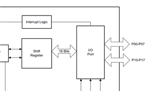
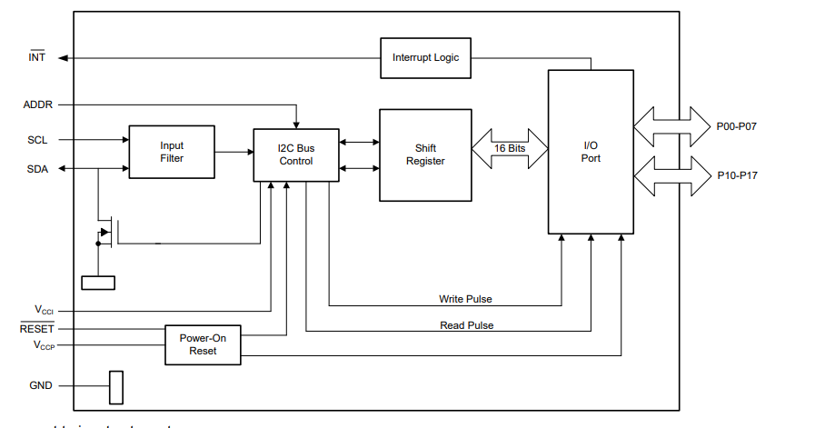
Let me ask about output timing for each output port.
Are the logic changes of output ports 00 to 17 at the same timing?
Or will the timing be divided between 00-07 and 10-17?
best regards
TATSU
Part Number: TCAL6416
Hi Team
Let me ask about output timing for each output port.
Are the logic changes of output ports 00 to 17 at the same timing?
Or will the timing be divided between 00-07 and 10-17?
best regards
TATSU