A related question is a question created from another question. When the related question is created, it will be automatically linked to the original question.
If you have a related question, please click the "Ask a related question" button in the top right corner. The newly created question will be automatically linked to this question.
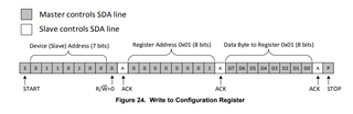
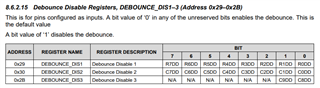
If you desire to write data to the debouncing registers, then you would need to follow the data format listed in figure 24 with correct device slave address, register address (either 0x29, 0x30, 0x2B), and the data you want to put into the register.
Configuration of these registers is done via the I2C bus on pins 23 and 22.
FYI,
a bit value of 0 enables the debounce feature for that row/col pin, this is the default value.
This has nothing to do with the previous question.
The code looks correct. What are the offset/value values you're calling this function which, and what is the desired effect, and what actually happens?