Part Number: DP83TC813R-Q1
hello
can you please advise the points below. the first 2 are info on signal customer didn't find in datasheet. the rest are timing that may require clarification:
- RGMII RX[3:0]: Vout_H and Vout_L
TX[3:0]: Vin_H and Vin_L
- MDI output common mode voltage: Vout_H and Vout_L
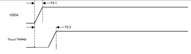
- How to understand T5.2? what is the delay offset for all supplies?
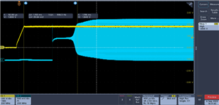
- How to capture T5.6? Is there a sign or mark that shows strap latch-in occurs? I want to measure T5.6
- T5.7 means which CLKOUT for DP83TC813R?
- Is there a sign or mark for idle stream start-up? Can I capture the sign or mark to measure T5.6?