


Other Parts Discussed in Thread: TCA9517
hi,
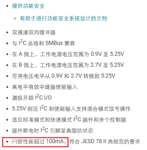
1. As shown in the following figure, how is the latch triggered? Can it be restored? If the latch is triggered, how can the chip electrical signal be determined?
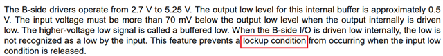
2. As shown in the following figure, how to understand this sentence with the word 'lock up'?
Thanks!

