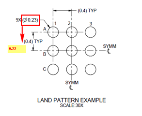
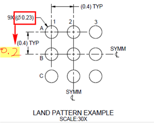
Part Number: TPD2S300
Hi Expert,
Do we know the substrate for the pin size(without ball)?
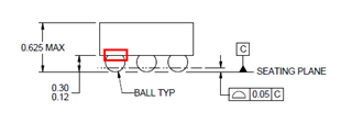
My customer can't do the via on pad(GND pin) on type 3 PCB, so they plan to reduce the footprint size for layout routing(0.23 to 0.22). Is there any side effect for reduce the ball?