This thread has been locked.

If you have a related question, please click the "Ask a related question" button in the top right corner. The newly created question will be automatically linked to this question.

DP83869HM: DP83869 Not powering ON Properly

Part Number: DP83869HM
Other Parts Discussed in Thread: DP83869

Hi,

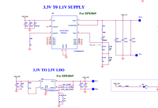
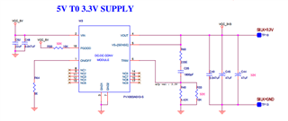
We are using DP83869 in  our design. Please find the schematics as per the attachment.

While powering ON our observation :

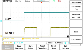
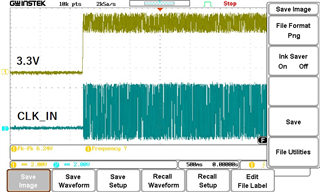
2.5V rail is getting 3.1V

When ALL RAILS are connected , at 3.3V we are getting 3.3v, BUT at 2.5V rail we have observed 3.1V. \

We have checked the source LDO 2.5V by removing the FB15.

We are getting 2.5V properly.

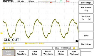
While debugging, in one card we have removed the DP83869, we are getting all voltages properly till the pads of U30.

When chipset is mounted condition, & FB15 removed in this point && When 3.3V RAIL alone connected irrespective external circuitry we are getting 3.1V at the  VDDA2P5_1

Please revert back for any queries. PLease support us
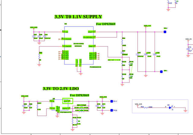
 

 Regards

Guru sai prasanth

  • Hi Guru Sai,

    Check power up sequence (Figure 11-2) in Section 11.1 Two-Supply Configuration (SNLS614B DP83869 Data Sheet) and see if it matches your design? 

    Is this happening on multiple boards?

    Attached is our Schematic Checklist, could you fill out the 'Customer System Overview' and 'Pin Wise Checklist" tabs please?

    7840.DP83869_Schematic_Design_Review_Checklist.xlsx

    Regards,

    Alvaro

  • Hi Alvaro Reyes

    We are powering ON all the supplies together (3.3V, 2.5V, 1.1V), as per mentioned in the data sheet.

    Please find the attached schematics for power sequencing.

    Is this happening on multiple boards?

    We have fabricated same chipset in many cards. In all cards (in this schematics) all the fabricated cards are showing same response. 

    Along with this, as we are using the same chipset from 2020, we are using with old datasheet. In old datasheet pin 23 strapping is not provided for double supply mode. And in earlier cards, the chipset is OPEN.All the cards are working fine. 

    But now as per the latest schematics is it mandetory for strapping pin 23. As we have pin 23 is floating? does it really affect the board?

    The old datasheet & new datasheets are attached.

    Regards

    Guru sai


  • Hi Guru,

    Supplymode_Sel Pin 23 is massive typo, please disregard

    Could you get a scope shot of the Power Up Sequence and when the issue is occurring?

    Is there any functional issue with the PHY because of this? No link, communication, etc.

    Regards,

    Alvaro

  • Hi Alvaro

    Please find the powerup sequence as per the attachment.

    3.3V & 2.5V rail with DP83869 CONNECTED. Once the DP83869 connected (FB15 is mounted, as per schematics), the voltage of 2.5V is shifting to 3.1V as per the below image. 

    We have even tried to connect the external load to 2.5V. If the load current is increasing to 2.5V rail, we observed the heating of DP83869 & voltage dipping from 3.1V to 2.6V, but in this situation, the chip is getting overheat.

    3.3V & 2.5V rail without DP83869 CONNECTED. FB15 is DNP/NM the voltage of 2.5V is not shifting as per the below image.


    3.3V to 1.1V rail. We have observed the clean 1.1V in all the observations.

    Is there any functional issue with the PHY because of this? No link, communication, etc.

    The chipset is not detecting by internal SAMAD536A Processor. No link, no activity establishing by the chipset.

    We have even Power ON the board with external supplies 3.3V, 2.5V, 1.1V. But still the same issue exists.

    We have even tried with connecting with the External MSP430 Board Via MDC, MDIO lines. Even with MSP430 Board, the chipset is not detecting.

    In another board we have removed the DP83869 chipset. In that card, we are reading 3.3V, 2.5V, 1.1V properly even at the PADs of DP83869. 

  • Hi Guru,

    Thank you for providing the supply ramps. I am not sure what is causing this issue, please allow me another day to consult with my team.

    Regards,

    Alvaro

  • Hi Guru,

    Could you probe the XI pin and confirm that is is getting a stable waveform before the power supplies are turned on?

    Could you also please fill out the 'Customer System Overview' and 'Pin Wise Checklist" tabs in the checklist?

    5751.DP83869_Schematic_Design_Review_Checklist.xlsx

    Regards,

    Alvaro

  • Hi Alvaro

    Please find the waveforms below

    i) 25Mhz clock

    ii) 25Mhz signal wrt Reset signal

    iii) MDC signal wrt 25Mhz signal

    Please also find the response for Pin Wise Checklist as per the attachment.

    5751.DP83869_Schematic_Design_Review_Checklist-done.xlsx

  • Thank you for the checklist Guru,

    I will review and provide feedback by end of week, Friday Sep 1st.

    As for the images, the clock signal doesn't look very clean. Are you using a scope that supports sampling in the 100 MHz range?

    Regards,

    Alvaro

  • Hi Alvaro

    Our scope supports 100Mhz range. 

    Whenever the time period is adjusted to  400m sec or 500 m sec range in the probe, the signal looks clean. Please find the below image.


    For analyzing the Reset signal (which requires 3-4  seconds) with respect to the clock signal, the range is set to 1 sec in the oscilloscope. Maybe because of this, the number of samples taken by oscilloscope is less & signal is not replicated properly.

    Regards

    Guru sai prasanth A

  • Hi Guru,

    I believe the PHY may be stuck, could you plot RESET/ XI / and Power in the same snapshot?

    Could you also probe CLKOUT separately? 

    Regards,

    Alvaro

  • Hi Alvaro,

    Please find the waveforms below

    i) Reset & Power

    ii) Power & clock

    iii) Clock output

    Regards

    Guru sai Prasanth A

  • Hi Guru,

    Thank you for the snapshots, I have a few other checks that I want you to check:

    • Confirm that CLK_IN is 25 MHz?
    • Probe RBIAS resistor and confirm that Voltage is 1V
    • Can you perform a Register Read and plot MDC & MDIO and confirm waveforms are per Section 9.4.9 Serial Management Interface`
      • Figures 9-13 & 9-14
    • Have you tried using a different DP83869 part? A known good part?

    Regards,

    Alvaro

  • Hi Alvaro,

    The CLK_IN & CLK_OUT are 25Mhz.

    The RBIAS voltage is 1V

    We tried to check the MDC, MDIO Lines.

    MDIO : 3.3V, MDC : 0V.

    We suspect the issue may be in the chipset, we are using the following chipset. Can you please check and confirm whether the chipset is fine or any damage?

    Regards

    Guru sai prasanth A

  • Hi Guru,

    From the picture all I can do is trace where this part came from. Have you tried replacing the part with another one?

    MDIO : 3.3V, MDC : 0V.

    MDC shouldn't be 0V, it should be a square wave signal, provided by the SOC. This would affect your ability to read/write registers but I don't think this is related to the 3.1V issue seen on the 2.5 V domain.

    Regards,

    Alvaro