Other Parts Discussed in Thread: ALP
Hi,
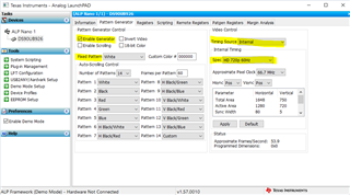
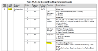
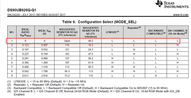
I working on an issue between De-Serializer(DS90UB926) and DLP3030. When we select the vertical test image (black and white strips), DLP output is in blue, and when we select the pattern generator in the ALP tool with the Vcom selection, it is also giving the blue color. we are suspecting that is about the calibration issue or the firmware issue in DLPC120
my setup:- DS90UB926->DLPC120->DLP3030
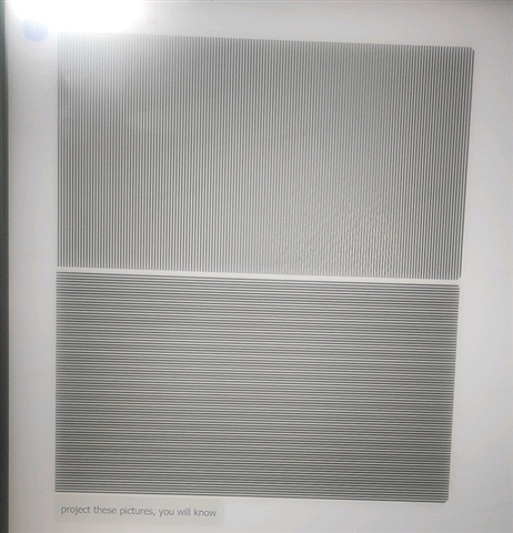
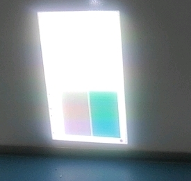
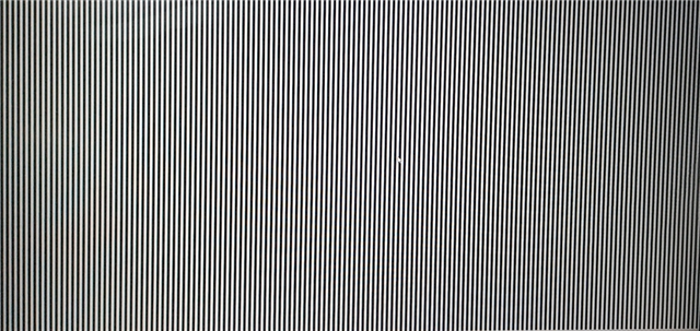
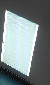
we are attaching our test images for the information, could you please suggest the better information for the clarity.