A related question is a question created from another question. When the related question is created, it will be automatically linked to the original question.
If you have a related question, please click the "Ask a related question" button in the top right corner. The newly created question will be automatically linked to this question.
DS90UB941AS-Q1: Schematic review(DS90UB941AS-Q1 and DS90UB940-Q1)
The customer's design review schedule is very tight, so I'm sorry but I hope that other engineer support this schematic review. Please forward it to someone else.
I will continue to review the sent schematics, estimated results by Friday. I appreciate your concern for timeliness, I will update you along the process.
An initial overview of the schematic I would like to confirm the IDx and mode selection. On page 1, the HUD_I2C_ADDR seems to be configured to R1 Open and R2 10.2 k-Ohm, which corresponds to 8-bit address 0x18.
Highlighted appears to be 0x1C, which would correspond to R1 and R2 requiring different values. Did you mean address 0x1C?
Thanks for an initial review of this case. The highlighted red box for IDX setting is something wrong on page 1. It is correct that strap resistors are R1 open and R2 10kohm. Also, please let me know that if other part's review is completed.
I will continue to update you as information is reviewed. Please allow me until next week to provide a sufficient amount of feedback regarding the entire schematic sent.
Some additional updates I would like to bring your attention to in the schematic:
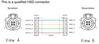
Review the HSD connection from the SER to the DES, this specific application of the pinouts is due to the differential cables twisting and changing orientation from View A to View B.
Since this is the scheme of the SER ports being used, it is recommended to ensure the pinouts of these are corresponding to the right places.
This is a reference to the pinouts used on other devices, ensure that the Link pinouts selected are following the recommendations, unless otherwise the cable is specifically routing the pins in a special manner. Do this for both the 941 and 940 connectors, ensuring the connections are consistent.
For the 941 devices, is there a common mode choke being used? This appears on the 940 but should be used at all FPD-Link connections before the HSD connectors.
For the DSI0 connections on the 941s, are these unpopulated resistors for the purpose of probing the high speed traces?
For the DSI1 connections on the 941s, please ensure that if these are floating to turn off the channel using the internal software assignments.
For the 941s, it seems the connection between both VDD18 and VDDIO pins are all connected, will there be a difference here between what is being used or are they all purposefully connected? Also, it may not be recommended to tie all nodes VDD_L through VDD11_DSI; P0, P1, HS0, HS1 are all sensitive pinouts and are not recommended to be connected to noisy voltage levels provided by VDD_L and power supply.
Please let me know if you have any further inquiries about the information above.
As I checked with the customer, their answers are as follows.
For the 941 devices, is there a common mode choke being used? Yes, there is no common mode choke on 941 because there is no part information on 941EVM. Can the choke(DLW21SN900HQ2L) be used on 941?
For the DSI0 connections on the 941s, are these unpopulated resistors for the purpose of probing the high speed traces? Do you recommend to delete these unpopulated resistors?
For the 941s, it seems the connection between both VDD18 and VDDIO pins are all connected, will there be a difference here between what is being used or are they all purposefully connected? Yes, all power pins of VDD18 and VDDIO are connected like 941EVM. Is there any problem?
Yes, there is no common mode choke on 941 because there is no part information on 941EVM. Can the choke(DLW21SN900HQ2L) be used on 941?
Although this part does show up on the EVMs, it may not be qualified for an automotive application, or AEC-Q certified. Take this into account when implementing passive components into the system, and find a suitable component to match the 100-ohm differential impedance while also being AEC-Q100 or AEC-Q200 certified.
Normally when common mode chokes are used, they are recommended to use for end-to-end connections of high speed signaling to reduce the effects of EMI. Either both devices should include it between the pinout and the connector, or neither should include it.
The recommendation here is to determine if your system requires using a CMC, otherwise it should be used on both SER and DES or neither. The drawback of including a CMC where it may not be necessary would be the additional impedance associated with the routing, but the resource listed here will be able to help you determine if this is right for your system: In-line and common mode chokes - use and effect on the transmission channel | Video | TI.com
Do you recommend to delete these unpopulated resistors?
This depends on how they are planned to be used. The high-speed traces may have further impedance with the introduction of pads for the unpopulated resistors, which could disturb the high-speed signaling coming through the DSI0 channels. Unless they are purposefully designed for probing or another application, they may be adding non-ideal impedance to the traces. Please validate the 100-ohm impedance requirements and if they are being met with these differential pinouts.
Yes, all power pins of VDD18 and VDDIO are connected like 941EVM. Is there any problem?
It looks like the nets of all the power for the VDD's are connected in the 941 and 940 chips. It may not be recommended to tie all the power pinouts at the output together due to power noise coming from the supply, and IR drops that may collect from the different sources routing to the same ferrite beads. For example, VDD18 and VDDIO rail going to the same BLM18PG121SZ1D may draw more current, leading to a larger IR drop. It is suggested to keep the VDDIO separate from the VDD18 pinout (under it's own VCC18 rail and ferrite bead) to avoid this.
On the right hand side, it seems the VDD11 may have been all connected together, which would tie all the capacitors together as well. From the design point of view, it may be recommended to keep these all separate paths. Additionally, BLM18PG121SZ1D may not be automotive compliant to use for an inductor, as it may not have the AEC-Q100 or 200 requirement needed for an automotive application. Be sure to verify this when selecting the LCR components for the design.
We recommend these implementations but please verify with your system that the required impedance specifications are being met according to the datasheet.
The application of the devices with these recommendations should be sufficient for the design of the schematic, but I will also continue to review the connections and component selection. As a reminder, ensure the AEC-Q automotive qualifications for all passive components if they plan to be used in the automotive environments.
Specifically, I would like to bring attention to sections 8.2 - Typical Applications on both datasheets, and also keep in mind Section 10 for future layout implementations.
Have the HSD connectors been verified end to end with continuity? This would also help evaluate whether the correct pinouts are placed between the connectors and the FPD devices.