This thread has been locked.

If you have a related question, please click the "Ask a related question" button in the top right corner. The newly created question will be automatically linked to this question.

Help with noise on a half-duplex M-LVDS line

Other Parts Discussed in Thread: SN65MLVD204, SN65MLVD206, SN65MLVD204A

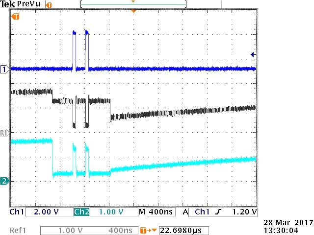
Hi, i am developing a half-duplex multipoint network based on M-LVDS. For now i am using just 2 nodes on the network, with a 30cm  Cat5e cable, 100Ohms termination on both ends. The boards were hand prototyped so  the tracks are not impedance matched.. but the max data rate i am using is 50Mbps and the max track lenght is about 2cm. The communication signal is being genarated by FPGAs on both side. I am driving DE ande RE pins with a single signal at both ends. The M-LVDS tranceivers are SN65MLVD206 and SN65MLVD204 (both type-2). 

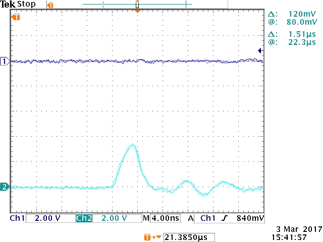
My problem is the following. When i put the DE/RE signal from high to low level a small pulse is generated on the receivers line. During this time, the differential line is floating, but i belive that is not the reason due to the type 2 failsafe and the line stays floating longer than the pulse. The LVTT lines are not Pulled Up or Down and the signal is alwyas on low logic level before disasserting DE/RE. Any ideal of the reason of this noise? Would leave the RE always on GND (Receiver active) solve this problem? If yes.. that is workable as i can just ignore any signal on the receivers line on the FPGA.

This pulse looks almost the same on every transition, so is not a noise source.. 

PS: To look at the signals i am using a 1Ghz scope, but as my probes are not well trimmed, the differential signal is very noise when i subtract both lines...

Thank you!

  • Hi Luis,

    Let me first make sure I understand the issue.  When you are swapping the direction of data flow by disabling the driver and enabling the receiver, you see a pulse on the device's "R" output pin.  This pulse always shows up, even when the bus (connected to pins "A" and "B") was driven low prior to enabling the receiver.  The same issue occurs with both the SN65MLVD204 and the SN65MLVD206 device.  Is this correct?

    There are a couple of things you might want to check:

    1. Does the pulse still show up when the cable is not connected?  The reactive properties (inductance and capacitance) of the cable may be causing some ringing when the line suddenly becomes high impedance.  It would be nice if you could look at the differential signal on an oscilloscope to verify this as well.  There may be less noise if you try looking at the differential signals individually (i.e., as single-ended signals) rather than subtracting them.
    2. Is it possible to install a pull-down resistor on the "R" output?  If there is no pull-down resistor, that node will be floating and relatively small leakage currents may be able to establish a high-level voltage on the line.

    Also, can you describe the pulse a little more - what is the magnitude and duration?  It would be helpful to see an oscilloscope screenshot if you have one.

    By the way, the SN65MLVD204 device is not recommended for new designs.  It has been replaced with the SN65MLVD204A.

    Best regards,
    Max Robertson
    Analog Applications Engineer
    Texas Instruments
    m-robertson@ti.com

  • Thank you for your reply Max.

    Yes, your description is correct, and actually the pulse appears at both receivers. I am not on the lab now and unfortunally my scope is a TDS784A, so just an old floppy as output... But the pulse is about 7-9ns wide.. maybe less... The magnitude is somewhat close to 3V (the same as the logic level High).

    I tryed to tie the Receiver Enable pin to ground but did not work. I looked at the scope, and was able to see a resonoable differential signal (subtracting both as my probes are active but not differential). There is a small ring right after the switch, but as i measured it does not go bigger than 50mV.. however as i told the probes are old and sometimes is impossible to calibrate them on the scope. I solved the problem adding bias resistors as mentioned on SLLA119, however i am using 400ohms resistors on a single end just for tests. Probably i am using  SN65MLVD204A as i bought it like 10 months ago at farnell, anyway.  What surprises me is that the failsafe does not works even on the rise from negative level to idle on the differential line.. and thats on a point-to-point line... Using the bias is there any difference on using type-1 or 2 receivers? Am i going to have any drowback using the bias? 

    Thank you!!

    PS: I am writing an article right now but i will probably get back to tests on friday... 


  • Luis,

    Using external pull-ups and pull-downs on the bus seems to me to be a good solution.  It will hold the line to a well-defined level when undriven so it should be less susceptible to noise.  It should also help with any overshoots that may cause glitches when the driver is disabled.

    Type 1 receivers have positive-going and negative-going switching thresholds that are set around 0 V differential.  Type 2 receivers have a single switching threshold (i.e., no hysteresis) that is set somewhere between +50 mV and +150 mV differential.  Adding an offset to the differential input of a Type 1 receiver will make it behave like a Type 2 receiver with hysteresis.  Removing the differential offset from a Type 2 receiver will make it behave like a Type 1 receiver without hysteresis.

    It sounds like you are using 400-Ohm pull-ups and pull-downs, which with 50 Ohms of bus loading will add a differential offset of about 200 mV.  If the polarity of this offset is negative (to hold the bus low when idle), then the received differential signal will need to have a "high" level greater than 350 mV (to account for the external offset of -200 mV and the maximum Type-2 switching threshold of +150 mV).  As long as your signal swing is high enough to reach this level (after accounting for loss through your transmission line), then it should work fine.  If you need more margin, you can try decreasing the amount of offset by increasing the resistance values.

    Please let me know if this does not make sense.

    Best regards,
    Max Robertson

  • Max, thank you for your response.

    Yea that's all correct. I was only concerned about the load on the bus and how the bias could affect it... I was seizing the circuit to a maximum 11 nodes on the bus so i am not sure if that is going to be possible... i am not expecting a great loss as the total distance wont be greater than 5m.. and probably not even 3m on Cat5 cable and transmission frequency wont go higher than 50Mbps.. All the nodes will be on  a daisy-chain fashion with a max stub of 2cm.

    This -200mV number i got from SLLA119, but there they used a 750 Ohms resistors at both ends resulting on a 375 effectively. My terminator is a RJ45 plug so biasing on both ends is not a direct task, but is doable as i have power distribution on the remaining pairs of the Cat5 cable...

    Thank you for your help.. any further comment will be apreciated.


    Luis Filipe Rossi

  • Luis,

    These M-LVDS devices have fairly large signaling swings, so in this application I don't think that adding a 200 mV offset will hurt performance much.  You can try it out in the lab (or in simulation) to see how much margin you can expect after accounting for loss.  You can always adjust the pull-up/pull-down resistances to give yourself more margin if needed.  I agree that you will most likely be fine as-is given the lower data rate and relatively short transmission distance.

    One thing to keep in mind is that shifting the threshold point away from 0 V (the differential crossing point) will result in some amount of pulse width distortion on the output.  You should make sure that this does not have an adverse effect on your system.  For example, if you have very strict set-up and hold requirements you might want to reduce the offset applied to the signal to make sure timing margins are not reduced.

    Best regards,
    Max Robertson

  • I am having the exact same problem as Luis. I am using the 65MLVD206 and tried briefly with the 65MLVD201 to see if it was better. My setup has a transmitter at one end (switched on and off via TE), 10 cm of transmission line, and a receiver at the other end. *RE is tied low at both ends. Each end has a 100 ohm terminator.  I need R at the receiving end to look exactly like D at the transmitting end. I will show you what I found on the scope:

    1: signal at D on transmitting 65MLVD206

    R2: signal at R on receiving 65MLVD201 (not really usable)

    2: signal at R on receiving 65MLVD206 (this has the glitch when TE is turned off)

    R1: signal at DE on transmitting 65MLVD206

    Zooming in on the glitch on the R line (the bottom trace):

    and looking at the LVDS A and B lines:

    1: signal at D on transmitting 65MLVD206

    R1: signal at B on receiving 65MLVD206

    2: signal at A on receiving 65MLVD206

    From this you can see that the LVDS signals behave. When TE is turned off, the B signal rapidly drops, and the A line moves up slightly but still B>A so we should not see a 1 output.

    It seems if I go to a 50 ohm termination instead of 100 ohm the problem goes away. I can also bias as Luis did, but it seems something is fundamentally wrong. I want a robust solution, and I fear this is a band-aid solution.

    Are you able to explain what is happening? Does the receiver have some inductance such that when B drops rapidly with A rising that it sees this as a 1, even though the voltage levels don't justify this?

    Thanks,

    Earl