This thread has been locked.

If you have a related question, please click the "Ask a related question" button in the top right corner. The newly created question will be automatically linked to this question.

TCA9617B: I2C multiple slave design

Part Number: TCA9617B
Other Parts Discussed in Thread: INA238, , TCA9517, TCA9509, SN74LV4052A, TCA9546A, TCA9511A

Hi,

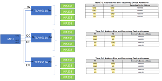
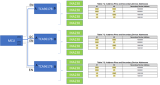
We need to interface twelve numbers of INA238 to MCU. Scheme selected is using TCA9617B (Four INA238 ICs as a channel, with same slave address). One TCA9617B will be enabled at a time. Can you please check the below scheme and share your feedback?

Regards,

Sneha

  • Hi Sneha,

    Unfortunately, the logic low input on the digital side of the IN238 is not high enough when implementing the TCA9617B. 

    From the datasheet, we can see that the logic low input level is a MAX of 0.4V. 

    The typical output logic low from the TCA9617B is 0.53V.

    This means that the INA238 would not be able to see a logic low input since the B-side output of the TCA9617B would not be able to output a voltage lower.

    Since the customer is only enabling a single TCA9617B at any given time, it might be okay to connect the B-sides of the 9617B together as long as only one buffer is active at any given time. This would also depend on the voltage levels of the MCU and the INA. There is also the risk of having more than one TCA9617B turn on at the same time which could cause data to be lost due to static voltage offsets being connected to each other. 

    TCA9517 would have similar issues. 

    I can think of two possible devices that could potentially solve this issue. One would be the TCA9509, which instead of a SVO to prevent bus lock up, there is a integrated current sense to determine which side is driving low. This means that multiple A-sides of the TCA9509 cannot be connected together, similar to the TCA9617B multiple B-sides cannot be connected together. I believe implementation of TCA9509 would work if the voltage supplies of the MCU and INA work. What are the voltage levels of these two components? 

    Another device to consider that has low output low voltage VOL is the TCA980x series. TCA980x has very low VOL which would be good for the input of the INA238. It requires that the design have no external / internal sources of current on the B-side. Things like pull-up resistors or leaky ESD structures on the B-side are not allowed for the TCA980x. This device also has level translation, and comes in different ICS current strengths. 

    Regards,

    Tyler

  • If you do not need buffering (i.e., if the total capacitance of the bus is small enough), you can also use passive switches to disconnect bus segments. The TCA9546A is controlled through I²C; general-purpose switches like the SN74LV4052A are controlled with GPIOs.

  • Hi Tyler,

    Thank you for your detailed reply and explanation on this.

    From the MCU side, I2C electrical specification is shown below:

    We are using a 3.3V power supply for the MCU as well as for the INA238 ICs and no need for the voltage level translator. Our concern on the design is the number of slave devices coming on the I2C bus. We need to connect 12 INA238 devices. There is a post regarding the I2C address select restriction with SDA pin.

    https://e2e.ti.com/support/amplifiers-group/amplifiers/f/amplifiers-forum/1182996/ina231-restrictions-by-slave-address-setting

    What is your feedback on the scheme using TCA9511A, where the Vol max is 0.4V.

    I can see that offset voltage of 0.1V (max) is there, and  if VOL is maximum, on the buffer output VOL can go upto 0.5V. Can you share your thoughts on this?

    Regards,

    Sneha

  • Hi Sneha,

    What is your feedback on the scheme using TCA9511A, where the Vol max is 0.4V.

    I can see that offset voltage of 0.1V (max) is there, and  if VOL is maximum, on the buffer output VOL can go upto 0.5V. Can you share your thoughts on this?

    The low-level output voltage spec shows that with an input Vin = 0.1V, the VOL(max) < 0.4V. This would include the offset from VIN to VOUT based on the VOS spec that you mentioned. The VOS does not add onto the maximum of VOL. 

    So TCA9511A from a datasheet perspective would guarantee by the electrical specifications an output <0.4V if the input Vin <= 0.1V. There might need to be an adjustment of the pull-up resistors on the MCU side to further guarantee that the input does not exceed 0.1V. 

    I did want to mention Clemens' comment on the idea of using a switch instead of a buffer. If capacitance is not an issue, consider using the TCA9546A, which is an I2C controlled switch that has 4 configurable channels. If you are concerned about VOL or VOS of different buffers, then a switch could be a viable solution. 

    Regards,

    Tyler

  • Hi Tyler,

    Thank you.

    So, we are planning to use TCA9546A based design, as shown below. Thank you Clemens for the suggestion

    Regards,

    Sneha

  • Hi Sneha,

    This configuration would work just fine, considering that only one channel of the 9546a will be enabled at any given time. 

    This solution does require pull-up resistors on both sides of the 9546a. Please be sure to select the correct pull-up resistance value in order that the VOL is sufficient for the input low logic of the INA238. This application note here helps to determine these values. 

    Regards,

    Tyler