This thread has been locked.

If you have a related question, please click the "Ask a related question" button in the top right corner. The newly created question will be automatically linked to this question.

INA231: Restrictions by slave address setting

Part Number: INA231

Slave address setting can set 16 addresses depending on what is connected to A0 and A1 pins. (equivalent to 4bit)
There are four connection destinations: GND, VS (power supply), SDA, and SCL.
SDA and SCL are signals for I2C communication.

(1) When the address is specified using SDA and SCL, when is the address determined?
When specifying (write operation) to INA231, how long should I wait after VS rises?
(2) Please tell me whether the slave address does not depend on the logical values of SDA and SCL.
(3) If there are restrictions such as the rise time of the power supply VS, the rise time of SDA and SCL, please tell us what they are.

We are currently developing a board with three INA231s.
Each slave address is designed as A0=SDA/A1=GND, A0=SDA/A1=VS(3.3V), A0=GND/A1=VS(3.3V).
Please let me know if there are any hardware or software restrictions such as those mentioned above.

  • 1. An I²C transaction requires transitions on both SCL and SDA. I guess that A0 and A1 are sampled before and during the start condition.

    2. The datasheet tells you to connect the A0/A1 pins to VCC/GND/SCL/SDA. The device will work correctly if you have made these connections (and if SCL/SDA have valid I²C voltages).

    3. The address cannot be detemined until the I²C bus becomes active, so the power supply rise time does not matter.

  • Hello,

    1, This is the most logical way for the INA to do this (see answer above). I am not 100% certain but will confirm with the design team. This will take some time and I will get back to you as soon as possible.

    2, See above answer.

    3, On page 6 section 7.6 of the INA231 datasheet you will find the timing diagram for the INA231 based on communication speed you will need to take note of different SDA and SCL timing needs.

    There are no restrictions on the having three INA231s in your circuit with the A0/A1 configuration you mentioned. Software will be something I cannot comment on without knowing more about the controller you plan to use, but there usually is not a software limitation.

  • Hi Mr Clemens  and Mr Castrense

    Thank you  for your support.

    We made PCBs with 3 INA231 mounted on it.

    A0A1 is ① A0=SDA/A1=GND, ② A0=SDA/A1=VS(3.3V), ③ A0=GND/A1=VS(3.3V).

    When I checked the operation, I2C communication was not possible for ① and ②.

    Changing ① to A0=SCL/A1=GND and ② to A0=VS(3.3V)/A1=VS(3.3V) enables I2C control.

    Even CLK frequency of 100kHz was useless.
    Since it works when the slave address is changed, the I2C control format itself is not the cause.
    I think that the slave address cannot be recognized when it is set to SDA.

    There is a similar question NA231: About Address Pins and Slave Addresses
    In answer by Mr. Carolus
    The device detects shorts between the pins.The level of voltage does not matter.

    By arranging these
    When the I2C bus becomes active, sampling is performed to check the continuity of A0 and A1, and the connection destination (VS/GND/SDA/SCL) is determined.
    A slave address is determined.
    It seems to work.
    I have a question.
    ・Please tell me what kind of state you mean by being active.
    ・Please tell me how to determine the connection destination by sampling and how long it takes.

    The I2C control format first sends 7 bits of slave address and 1 bit to determine R/W.
    It seems that the connection destination of A0 and A1 is not decided (or is wrong) at the delicate timing here.

  • "Active" means some communication, i.e., SDA/SCL change between high and low.

    Connecting A0/A1 directly to SDA/SCL should work.

    Please show the schematic.

  • Hello,

    Using SDA as an address is fine in most cases but in rare situations it may lead to mis-identification, due to SDA timing variation.

    We suggest using the other options first. Use SDA only when other options have been exhausted.

    If changing to the configuration you have changed to is a long term possibility that will be the best option.

    As far as your questions question 1 was answered by Clemens, but more specifically a start condition.

    For your question 2 the minimum time for hold time after a start or repeated start would be 100ns.

    Regards,

    Cas

  • Hellow Mr.Clemens and Mr.Castrense

    Sorry for the late reply.

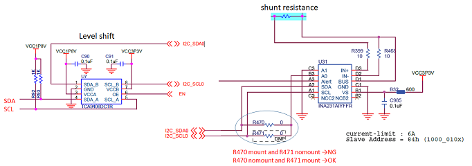
    I  attached the schematic.

     Mr Castrense.'s answer "in rare situations it may lead to mis-identification, due to SDA timing variation."

    About "in rare situations"
    (1) Occasionally misidentification occurs when the Board is in operation.
    (2) There is a possibility that some designed boards may be misidentified due to timing fluctuations.
    In this case, the board always fails to operate due to misrecognition.

    Which is (1) or (2)?

    The board we designed could not work I2C at all for INA231 with A0=SDA.

    Therefore, we think (2).

    Best regards.

  • Hello,

    There could be a resolution with the timing if you must use the A0 = SDA. So the first and easiest fix would be to not use SDA for the address pin. 

    You could also center the SDA data to the SCL low when sending data as well as the start condition. This should help the misidentification problem specifically it is important in the address byte.

    Regards,

    Cas

  • Hi Cas-san,

    Thank you for supporting Mr. Umehara on E2E. This is Itoh, AFAE supporting him.

    Could you please elaborate on the SDA timing variation more specifically?

    Mr. Umehara determined to avoid A0=SDA as workaround but he is still interested in the root cause of this issue.

    Regards,

    Itoh

  • Hello Kazuki Itoh,

    I sent you a private message.

    Regards,

    Cas