This thread has been locked.

If you have a related question, please click the "Ask a related question" button in the top right corner. The newly created question will be automatically linked to this question.

TCAL9539-Q1: 13.5V input sense

Part Number: TCAL9539-Q1
Other Parts Discussed in Thread: TCA9539-Q1, TCAL9539

Hi Expert, 

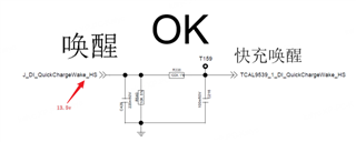
Customer is using one of the IO to detect 13.5V high level signal, you can find the portion of schematic as below. 

They placed a 100K series resistor before input to TCAL9539-Q1. I would like to check with you if the configuration is reasonable? Customer mentioned that this input pin damaged after the input 13.5V signal. After damage, they can always see 3.3V signal on this IO pin. 

Please help check if it can be used to sense 13.5V signal and how to design. 
Thanks!

Ethan Wen

  • Hi Ethan,

    It sounds like the customer used the device outside the absolute max conditions in the datasheet. The absolute maximum voltage that an input pin can handle for the TCAL9539-Q1 is +4V. The customer put a 13.5V signal on the port, which most definitely caused damage to the IC. If they are seeing 3.3V on the IO pin, they are probably reading the VCC voltage, since there is probably a short to VCC due to the over voltage damage. 

    My suggestion would be to alter this circuit by adding a resistive divider, not just a series resistance. 

    What is the 10kohm resistor doing? This 10k does not form a correct resistive divider before the input of the IO expander. The resistor needs to be moved or removed entirely. Also, a 10kohm pull-down resistor after the 100kohm resistor would yield an output voltage of 1.227V, which is to low for a high logic signal. A logic high by I2C standards is VCC * 70%. If VCC = 3.3V, then VIH(min) = 2.31V. Therefore, the 10kohm would need to increase in resistance. 

    Regards,

    Tyler

  • Hi Tyler, 

    May I know if there have clamping diode inside of IO pin? If yes, what is the clamping voltage? What is the maximum current capability? Is it 20mA? If yes, (13.5V-4V)/100K=95uA, it won't damage the clamping diode.  

    Thanks for the suggestion. 

    Ethan Wen

  • Hi Ethan,

    In section 6.5, there is a spec concerning the input diode clamp voltage that states a current draw of -18mA will generate a negative voltage of -1.2V on the input pin. 

    In the absolute maximum conditions, the maximum allowed input/output clamping current is -20mA.

    The maximum input voltage seems to disagree with section 6.5, but if you read the footnote (2) next to the abs. max input voltage, it states "The input negative-voltage and output voltage ratings may be exceeded if the input and output current ratings are observed. It appears that the clamping diode is only present only on a negative input side. I don't believe there is a clamping diode from the input to VCC. 

    Where is the customer getting the 4V from? I believe the math provided does not work out due to the capacitance present on the input. Overtime, C216 + the input cap from the input pin of the IO expander will charge up through the 100kohm at the rate of the RC time constant to 13.5V. This energy is stored in the cap. The input effectively sees 13.5V, and energy is dissipated into the IC with a voltage of 13.5V, not 4V. This voltage present at the input is way outside the absolute maximum input voltage, and I would assume that the high voltage input is the reason for the damage. 

    Regards,

    Tyler

  • Hi Tyler, 

    Thanks for the detailed reply. 

    May I know the high level/low level input voltage threshold for TCAL9539? I cannot find in datasheet. But I find it is 0.7VCC for high level input from TCA9539-Q1. Can you help confirm? 

    Another question, customer feedbacked that it is hard to select the suitable resistor divider value in this case. So they would like to add 3.3V clamping diode externally. Are there any design considerations need to attention? 

    Regards, 

    Ethan Wen

  • Hi Ethan,

    It looks like we did not include the input voltage thresholds in the TCAL9539 datasheet, but they should be the same as the thresholds found in the TCA9539-Q1 datasheet. These values come from the 70% 30% voltage levels rules from the I2C standard. 

    VIH = 70% of VCC

    VIL = 30% of VCC

    Will be true for the SCL, SDA, A0, A1, /RESET, P00-P07, and P10-P17 voltage input thresholds. 

    Another question, customer feedbacked that it is hard to select the suitable resistor divider value in this case. So they would like to add 3.3V clamping diode externally. Are there any design considerations need to attention? 

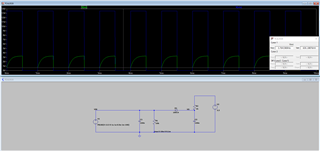
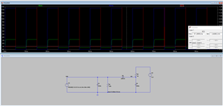
    I created a simple schematic using a diode in replacement of the 100k series resistor. Is this the idea that the customer has? 

    This is one way to level shift, but the voltage on VO when a logic low occurs is V = 630mV. If using a 3.3V supply, this means that the 30% logic level input is 

    30% of VCC = 0.99V. 

    This would work since the input to the IO expander is 0.63V, which is well below the VIL(min) of 0.99V for a 3.3V supply. 

    Design considerations would be value of R2 pull-up resistor. This needs to be adjusted in order to control the rise-time of the input. It is also responsible for limiting the current through the diode. 

    In this example, you can see that the current through the forward biased diode when the input supply is logic low is 2.67 mA at a diode drop of around 0.63V. This would be an okay power dissipation for a diode such as 1N914. 

    Also check current through R1 resistor to ensure all components can handle the amount of power being dissipated. 

    Regards,

    Tyler