Part Number: DS90UB941AS-Q1
Other Parts Discussed in Thread: ALP, USB2ANY
Hi Team,
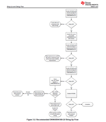
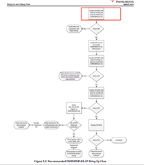
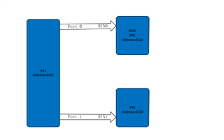
A simplified connection diagram is shown below :
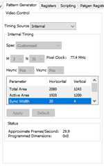
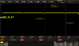
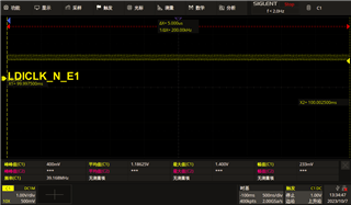
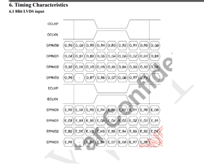
1.panel timing:
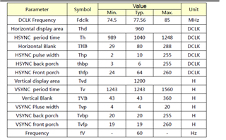
2.
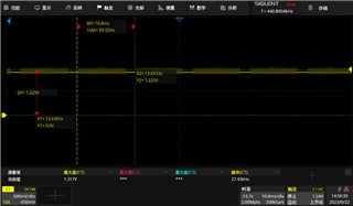
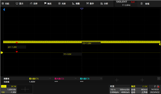
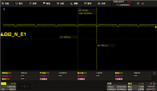
I used the 941AS splitter mode but could not output the picture.
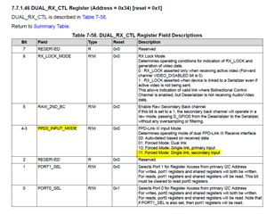
my script configuration is shown below,Please check whether the configuration is correct
{0x0c, 0x01, 0x02},
{0x0c, 0x01, 0x08},
{0x0c, 0x1e, 0x01}, //port0
{0x0c, 0x5b, 0x07}, //split mode
{0x0c, 0x4f, 0x8c}, //4lane contiune clk
{0x0c, 0x02, 0x06}, //data clk PN swap
{0x0c, 0x40, 0x04}, //DSI/DPHY port0
{0x0c, 0x41, 0x05},
{0x0c, 0x42, 0x2e}, //dsi clock 438,
{0x0c, 0x41, 0x20},
{0x0c, 0x42, 0x6f},
{0x0c, 0x56, 0x80}, //left/right split
{0x0c, 0x32, 0x80},
{0x0c, 0x33, 0x07}, //h 1920
{0x0c, 0x1e, 0x01}, //port0
{0x0c, 0x36, 0x00},
{0x0c, 0x37, 0x80},
{0x0c, 0x38, 0x7f}, //stop 1919
{0x0c, 0x39, 0x07},
{0x0c, 0x3a, 0x00},
{0x0c, 0x3b, 0x00},
{0x0c, 0x3c, 0xAF}, //stop 1199
{0x0c, 0x3d, 0x04},
{0x0c, 0x1e, 0x02}, //port1
{0x0c, 0x36, 0x00},
{0x0c, 0x37, 0x80},
{0x0c, 0x38, 0x7f}, //stop 1919
{0x0c, 0x39, 0x07},
{0x0c, 0x3a, 0x00},
{0x0c, 0x3b, 0x00},
{0x0c, 0x3c, 0xAF}, //stop 1199
{0x0c, 0x3d, 0x04},
{0x0c, 0x40, 0x10}, //DSI/DPHY port1
{0x0c, 0x41, 0x86},
{0x0c, 0x42, 0x0a},
{0x0c, 0x41, 0x94},
{0x0c, 0x42, 0x0a},
{0x0c, 0x1e, 0x01}, //port0
{0x0c, 0x03, 0x9a}, //pass_through
{0x0c, 0x1e, 0x02}, //port1
{0x0c, 0x03, 0x9a}, //pass_through
{0x2c, 0x1e, 0x09}, //port0 panel backlight
{0x30, 0x34, 0x19}, //Forced Mode: Single link, secondary input
{0x30, 0x1e, 0x09}, //port0 panel backlight
{0x0c, 0x01, 0x00}, //enable dsi