This thread has been locked.

If you have a related question, please click the "Ask a related question" button in the top right corner. The newly created question will be automatically linked to this question.

DP83825I: SOR1/SOR2 RX_DV inconsistent documentation

Part Number: DP83825I

I'm having a problem with RMII back-to-back repeater application and I'm trying to debug it.

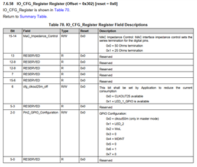
I'm trying to check whether PHY recognizes RX_DV bootstrap or not (reading SOR1 and SOR2 registers), but datasheet does not seem to be helpful and I'm looking for clarification.

Table 88 (SOR1) lists CRS_DV/RX_DV bit, but it is described as reserved. Table 89 (SOR2) lists CRS_DV_vs_RX_DV, but without any description (and relation between physical bootstrap state and bit state is not consistent between different bootstrap pins). In the datasheet of DP83826 similar bit is described to be set to 1 for RX_DV/back-to-back repeater mode, but in general this PHY registers look different. Would any of these bits (from either SOR1 or SOR2) be meaningful for DP83825I?

Overall DP83825I datasheet seems to be outdated - it was last updated in August 2019 while e.g. DP83826 had an update in November 2022.

  • Hi Tomazs,

    0x0468[11] should give you the value of the strap latched. 0x0302[8] should also give you the same value. 0x0302[8] also has an Read, Write option where writing the value will change whether the pin is RX_DV or CRS_DV.

    Description: 0b = CRS_DV, 1b = RX_DV.

    --
    Regards,
    Gokul.

  • Thank you! Setting undocumented bit 8 in IO_CFG helped. I'm not sure why hardware bootstrap was not working, I'll ask later for double-checking PCB under a microscope, though it is slightly weird as I have it on two PCBs.

    I have to say I'm developing distrust towards this datasheet, I'm counting 6 errors in the "Bit" column of table 70 alone: