This thread has been locked.

If you have a related question, please click the "Ask a related question" button in the top right corner. The newly created question will be automatically linked to this question.

DS90UB941AS-Q1: Using the SoC's DSI data and clock cannot light on the screen

Part Number: DS90UB941AS-Q1
Other Parts Discussed in Thread: SN65DSI83

Hi Team,

Based on the internal image generator, the screen can be lit. A simplified application diagram is as follows: 

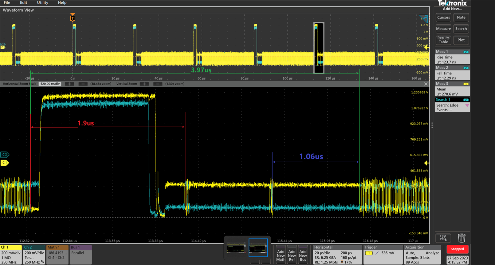
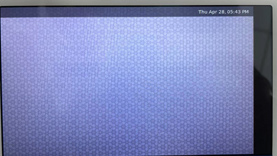
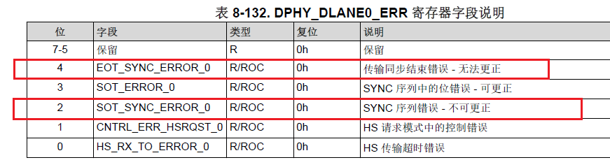
However, multiple attempts were made using the SoC's DSI data and clock and the screen still does not turn on. The DSI output is configured for video mode, burst mode, continuous clock mode. Through oscilloscope, it can be seen that the DSI can output normally. However, after the register configuration is performed, the screen still does not work. Checked DPHY related registers 0xF,0x10,0x11,0x12,0x13,0x14,0x15, status register values of all four data lane are 0x14 = 0001 0100, where bit2 and bit4 are indicated with errors: 

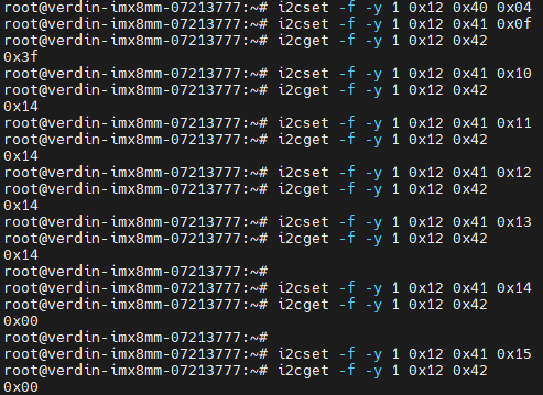
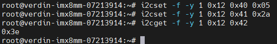
The register configuration is as follows: 

#!/bin/bash

# 800x480p60, Dual Link FPD III
# PCLK = 33.264MHz
# DSI clock = 99.792MHz
# DSI Lane Speed = 199.584Mbps/lane
# 4 Lanes DSI
# DSI input port 0
# DSI clock and DSI data
# use i2c-tools to debug

set -e

I2C_BUS_NUMBER=1
UB941AS_ADDR=0x12
UB928_ADDR=0x2c

# Disable DSI
i2cset -y -f -r $I2C_BUS_NUMBER $UB941AS_ADDR 0x01 0x08

# Select FPD-Link III Port 0
i2cset -y -f -r $I2C_BUS_NUMBER $UB941AS_ADDR 0x1e 0x01

# Enable I2C_PASSTHROUGH
i2cset -y -f -r $I2C_BUS_NUMBER $UB941AS_ADDR 0x03 0x9a

# Force select port 0
i2cset -y -f -r $I2C_BUS_NUMBER $UB941AS_ADDR 0x5b 0x21

# Select DSI Port 0 digital registers
i2cset -y -f -r $I2C_BUS_NUMBER $UB941AS_ADDR 0x40 0x04
# Select DSI_CONFIG_0 register
i2cset -y -f -r $I2C_BUS_NUMBER $UB941AS_ADDR 0x41 0x20
# Set DSI_SYNC_PULSES = 0
i2cset -y -f -r $I2C_BUS_NUMBER $UB941AS_ADDR 0x42 0x6f

# Select DSI_CONFIG_1 register
i2cset -y -f -r $I2C_BUS_NUMBER $UB941AS_ADDR 0x41 0x21
# Set DSI_VS_POLARITY=DSI_HS_POLARITY=1
i2cset -y -f -r $I2C_BUS_NUMBER $UB941AS_ADDR 0x42 0x60
#i2cset -y -f -r $I2C_BUS_NUMBER $UB941AS_ADDR 0x42 0x00

# Set DSI_CONTINUOUS_CLOCK, single DSI, 4 lanes, DSI Port 0 input
i2cset -y -f -r $I2C_BUS_NUMBER $UB941AS_ADDR 0x4f 0x8c

# DSI_HSW_CFG_HI
i2cset -y -f -r $I2C_BUS_NUMBER $UB941AS_ADDR 0x41 0x30
i2cset -y -f -r $I2C_BUS_NUMBER $UB941AS_ADDR 0x42 0x00
# DSI_HSW_CFG_LO hsync-len = 48
i2cset -y -f -r $I2C_BUS_NUMBER $UB941AS_ADDR 0x41 0x31
i2cset -y -f -r $I2C_BUS_NUMBER $UB941AS_ADDR 0x42 0x30
# DSI_VSW_CFG_HI
i2cset -y -f -r $I2C_BUS_NUMBER $UB941AS_ADDR 0x41 0x32
i2cset -y -f -r $I2C_BUS_NUMBER $UB941AS_ADDR 0x42 0x00
# DSI_VSW_CFG_LO vsync-len = 1
i2cset -y -f -r $I2C_BUS_NUMBER $UB941AS_ADDR 0x41 0x33
i2cset -y -f -r $I2C_BUS_NUMBER $UB941AS_ADDR 0x42 0x01

# TSKIP_CNT set DSI/D-PHY port0
i2cset -y -f -r $I2C_BUS_NUMBER $UB941AS_ADDR 0x40 0x04
# TSKIP_CNT set indirect addr (reg DPHY_SKIP_TIMING)
i2cset -y -f -r $I2C_BUS_NUMBER $UB941AS_ADDR 0x41 0x05
# TSKIP_CNT set reg DPHY_SKIP_TIMING value
i2cset -y -f -r $I2C_BUS_NUMBER $UB941AS_ADDR 0x42 0x04

# Initialize DSI clock settings (From Section 10.2 of datasheet)
i2cset -y -f $I2C_BUS_NUMBER $UB941AS_ADDR 0x40 0x10
i2cset -y -f $I2C_BUS_NUMBER $UB941AS_ADDR 0x41 0x86
i2cset -y -f $I2C_BUS_NUMBER $UB941AS_ADDR 0x42 0x0A
i2cset -y -f $I2C_BUS_NUMBER $UB941AS_ADDR 0x41 0x94
i2cset -y -f $I2C_BUS_NUMBER $UB941AS_ADDR 0x42 0x0A

# Enable DSI
i2cset -y -f -r $I2C_BUS_NUMBER $UB941AS_ADDR 0x01 0x00

1) Dose this error indicating the SoC's DSI output is not configured correctly? Or what else error?

2) Customer only configured 941 registers, is 928 deserializer also required additional configuration? 

Could you please help check this case? Thanks.

Best Regards,

Cherry

  • Hi Cherry,

    1) Dose this error indicating the SoC's DSI output is not configured correctly? Or what else error?

    Based on the registers its content is 0x14, there is a SYNC sequence error on each DPHY lane. Can the customer output PATGEN? Please take a look at section 3 in this app note: https://www.ti.com/lit/an/snla356/snla356.pdf?ts=1695335470653&ref_url=https%253A%252F%252Fe2e.ti.com%252F

    I would recommend to follow the flow chart provided in this app note as it gives a step by step to narrow down on the problem.

    Best Regards,

    Gil Abarca

  • Hi Gil Abarca,

    Thank you for the support!

    The customer's PATGEN results are as follows:

    • Internal clock and internal timing which can be normally displayed.
    • External clock and Internal timing which can be normally displayed.
    • External clock and external timing which is not able to be shown.

    What is the difference between enabling PATGEN and not enabling PATGEN using external clock and external timing as well? When PATGEN is enabled, the image displayed is the color bar or gradient pattern set; when PATGEN is not enabled, the image output by the SoM is displayed. The difference between the two is the difference in what is displayed, right? 

    Thanks and regards,

    Cherry

  • Hi Cherry,

    The customer's PATGEN results are as follows:

    • Internal clock and internal timing which can be normally displayed.
    • External clock and Internal timing which can be normally displayed.
    • External clock and external timing which is not able to be shown.

    The FPD-Link is configured correctly since the customer is able to generate PATGEN.

    Is the DSI_VD_DTYPE correct?

    What is the difference between enabling PATGEN and not enabling PATGEN using external clock and external timing as well?

    When PATGEN is enabled, the image displayed is the color bar or gradient pattern set; when PATGEN is not enabled, the image output by the SoM is displayed. The difference between the two is the difference in what is displayed, right? 

    You mentioned that the screen is not outputting the video. If PATGEN is not enabled, the screen outputs the video data is this correct? Can you clarify?

    Best Regards,

    Gil Abarca

  • Hi Gil Abarca,

    When PATGEN is enabled, the image displayed is the color bar or gradient pattern set; when PATGEN is not enabled, the image output by the SoM is displayed. The difference between the two is the difference in what is displayed, right? 

    You mentioned that the screen is not outputting the video. If PATGEN is not enabled, the screen outputs the video data is this correct? Can you clarify?

    Please let me clarify, this is only the assumption from the customer and you have replied with the image. Thank you.

    Is the DSI_VD_DTYPE correct?

    DSI_VD_DTYPE cannot be found, while the customer just found DSI_VC_DTYPE register. Is this a typo? If not, could you help tell where can we find it? 

    After configuration, DSI_VC_DTYPE reads as 0x3e: 

    Thanks and regards,

    Cherry

  • Hi Cherry,

    DSI_VD_DTYPE cannot be found, while the customer just found DSI_VC_DTYPE register. Is this a typo? If not, could you help tell where can we find it? 

    After configuration, DSI_VC_DTYPE reads as 0x3e: 

    You are correct, there is a typo it should be DSI_VC_DTYPE.

    The lower 4 bits of the DSI Data type should range between 0xB to 0xE. Data collected in customer's system demonstrate that this is correct the lower 4 bits are 0xE.

    We can move forward to the next step "Check Section 4.4 to verify TSKIP_CNT". The code shows that the TSKIP value is 0x04. I did the calculation using the equation (TSKIP_CNT = (65 * 0.099792 - 5) << 1) provided in the app note and it should be 0x2. Can you test this in the customer's system?

    Best Regards,

    Gil Abarca

  • Hi Gil Abarca,

    I did the calculation using the equation (TSKIP_CNT = (65 * 0.099792 - 5) << 1) provided in the app note and it should be 0x2. Can you test this in the customer's system?

    They've changed the original setting of 0x4 to 0x2, but the screen still cannot be lit on.

    Thanks and regards,

    Cherry

  • Hi Cherry,

    Can the customer follow steps 4.3 + 4.6 and send me the data for each section?

    Best Regards,

    Gil Abarca

  • Hi Gil Abarca,

    4.6: Burst mode is used, so DSI_sync_pulses in the DSI_config_0 register is set to 0:

    # Select DSI Port 0 digital registers
    i2cset -y -f -r $I2C_BUS_NUMBER $UB941AS_ADDR 0x40 0x04
    # Select DSI_CONFIG_0 register
    i2cset -y -f -r $I2C_BUS_NUMBER $UB941AS_ADDR 0x41 0x20
    # Set DSI_SYNC_PULSES = 0
    i2cset -y -f -r $I2C_BUS_NUMBER $UB941AS_ADDR 0x42 0x6f

    The source signal parameters are as follows: 

    HACT = 800
    HFP = 40
    HBP = 40 
    HSW = 48
    HTOTAL = 928
    VACT = 480
    VFP = 13
    VBP = 31 
    VSW = 1
    VTOTAL = 525

    The HSW and VSW registers are also set as required:

    # DSI_HSW_CFG_HI
    i2cset -y -f -r $I2C_BUS_NUMBER $UB941AS_ADDR 0x41 0x30
    i2cset -y -f -r $I2C_BUS_NUMBER $UB941AS_ADDR 0x42 0x00
    # DSI_HSW_CFG_LO hsync-len = 48
    i2cset -y -f -r $I2C_BUS_NUMBER $UB941AS_ADDR 0x41 0x31
    i2cset -y -f -r $I2C_BUS_NUMBER $UB941AS_ADDR 0x42 0x30
    # DSI_VSW_CFG_HI
    i2cset -y -f -r $I2C_BUS_NUMBER $UB941AS_ADDR 0x41 0x32
    i2cset -y -f -r $I2C_BUS_NUMBER $UB941AS_ADDR 0x42 0x00
    # DSI_VSW_CFG_LO vsync-len = 1
    i2cset -y -f -r $I2C_BUS_NUMBER $UB941AS_ADDR 0x41 0x33
    i2cset -y -f -r $I2C_BUS_NUMBER $UB941AS_ADDR 0x42 0x01

    4.3: the customer do not have a DSI analyzer and they use an oscilloscope to capture the waveform of lane 0 as follows: 

    Thanks and Regards,

    Cherry

  • Hi Cherry,

    I will review the data and get back to you by the end of the day tomorrow.

    Best Regards,

    Gil Abarca

  • Hi Cherry,

    It looks like the LP-11 transition is happening during the HFP. The DSI source may not have enough time to transition between HS->LP->HS between ending the video line long packet and sending the HSS packet. 

    This can be used as a potential solution:

    Can you probe the HS/VS/DE signals that the 941 is receiving? Once the data has been collected send the saleae capture.

     Procedure that needs to be done:

    1. Ensure VDDIO is 3.3V
    2. Write 0xB6 to register 0x24
    3. Probe GPIO 14, 38, and 39 with a Saleae
    4. GPIO 4 = Data Enable, GPIO 38 = VSYNC, GPIO 39 = HSYNC

    Best Regards,

    Gil Abarca

  • Hello All,

    Per our discussion today here is some feedback on this case:

    1. I re-reviewed the script. From the script analysis it seems like you are actually configuring the 941AS for DSI event mode vs. pulse mode because you are configuring DSI_SYNC_PULSES = 0. This is ok to do, but may not be required since it seems like your SoC may already be sending both HSS and HSE (pulse mode). 

    But I see one issue which is that in event mode when you override the timings, there is one known documentation error for the 941AS that the override value for DSI_VSYNC_WIDTH must be +1 from the desired value. You can see more info about that previously discovered issue here: https://e2e.ti.com/support/interface-group/interface---internal/f/interface---internal-forum/1116357/ds90ub941as-q1-need-help-to-complete-review-script-for-2-2-independent-mode 

    So for the script you would want to make the following modification:

    # DSI_VSW_CFG_LO vsync-len = 1
    i2cset -y -f -r $I2C_BUS_NUMBER $UB941AS_ADDR 0x41 0x33
    i2cset -y -f -r $I2C_BUS_NUMBER $UB941AS_ADDR 0x42 0x02

    That modification may actually resolve your display issue because with the current configuration I don't believe you will be getting any Vsync pulse, but to be clear it will not correct 100% of the timing issue you have here from the DSI source. So if the above does not resolve your issue we will have to look deeper at correcting the SoC timing issue by #2

    2. For the SoC timing issue, I've attached a spreadsheet showing the calculated timings which should be coming from the SoC between different DSI packet events, compared with the measured values to show the difference. The main point is that the HFP value is >> than expected because the SoC driver is trying to insert an LP11 pulse in the HFP but there is not enough time to do so and still maintain video DPI timing that you expect. So the effect is that HFP is too long and HSW is too short compared to your expected values. This can only be addressed via the SoC configuration. See section 4.3 of the DSI Bringup App Note for detailed info on this phenomenon 

    941AS Timing Calcs.xlsx

    https://www.ti.com/lit/pdf/snla356

    Best Regards,

    Casey 

  • Hi Casey ,

    Appreciate your feedback and support here!

    Without modifying the DSI source, the customer has modified some of the contents in the drive of 941, combined with the register modifications provided, and can now successfully illuminate the screen using the DSI.

    However, the picture of the screen is shifted all the way to the left, and there is a black block on the right, as shown below:

    The same screen used the same timing on the sn65dsi83 and the picture is normal. The DSI input source for both devices also remains the same.
    The problem can also be corrected by adjusting the HBP value to large in the device tree as follows:

    The customer would like to know what could be causing this? Is it due to there is some difference in resolution between 941 and sn65dsi83? 

    Thanks and regards,

    Cherry

  • Hi Cherry,

    Is it due to there is some difference in resolution between 941 and sn65dsi83? 

    These two devices are different and their configuration is different. 

    The customer would like to know what could be causing this?

    The expected HBP is 40. What is the modified HBP?

    Best Regards,

    Gil Abarca

  •  Hi Gil Abarca,

    The expected HBP is 40. What is the modified HBP?

    HBP value used on sn65dsi83 is 40 and modified HBP on 941 is 92 to display in the correct location.

    Thanks and regards,

    Cherry

  • Hi Cherry,

    Based on the image shared in this thread the LP-11 transition might be happening during the HFP. The expected blanking parameters are HFP = 40, HBP = 40, and HSW = 48. There still could be some HFP but not 40 pixels as expected or enough pixels to meet the blanking requirements of the display. Therefore, by adding that missing blanking to the HBP it compensates the total blanking required by the display.

    Best Regards,

    Gil Abarca