This thread has been locked.

If you have a related question, please click the "Ask a related question" button in the top right corner. The newly created question will be automatically linked to this question.

Regarding the serious problem of signal quality reflection at intermediate nodes when multiple SN65MLVD201 devices are connected to the bus

Other Parts Discussed in Thread: SN65MLVD201, DS90LV001, DS10BR150

Hi,

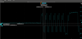
     My design is to have a bus backplane with 10 cards inserted on it. Each card has a bus interface chip SN65MLVD201 device, and there are 100R termination resistors at both ends of the bus. The bus received by the card in the middle slot has poor signal quality and severe reflection, which leads to signal recognition errors. I would like to ask if there is any optimization solution

     Looking forward to receiving a reply!

     Best Regards!

     Beryl


  • What are the lengths of the stubs? If they are too long, you might need a buffer like the DS90LV001 or DS10BR150.

  • Hello Beryl,

    Generally, you will get a worse signal performance in the middle slots since these cards are further away from the termination resistor.

    Like Clemens mentioned, things like stub length, slot spacing, characteristic impedance can play a role in having poor signal quality.

    We do have a video on how to properly design for M-LVDS (Designing with M-LVDS in Backplane Applications)

    Regards,

    Josh

  • Hi,

       Our structure is limited,slot sapceing is regular,and We test the differential signal waveform and Chip single ended output as shown in the following figure


  • What is the length of the stub from the backplane bus to the slot's receiver?

  • The total length is Nearly 2 inches,Two connectors have passed through it,Structure as shown in the figure

  • Hello Beryl,

    Is there a possibility to reduce the stub length? Additionally, what is the characteristic impedance the board was designed for?

    Regards,

    Josh

  • Hello Josh,

         It can reduce the stub length,but not much and the characteristic impedance was designed for 100Ω.

     Additionally, Look at the waveform I uploaded, it's the SN65MLVD201D received differential signal ,the low-level time has nearly 9ns,The low-level time of the differential to single end output signal has been reduced by 7ns,This single ended signal is sent to the FPGA, and the low level received signal by the FPGA needs to be ≥ 7.5ns.

  • Hello Beryl,

    Yes, if the stub length can be reduced even more that would be better for signal integrity. 

    Generally you want the characteristic impedance to be higher than the typical 100Ω. Reason is when you are loading the backplane with cards, the effective impedance will be much lower. A good rule of thumb is to have a characteristic impedance of 130Ω.

    Most likely when 10 cards are loaded, your effective impedance won't match the termination resistors. You could lower the termination resistor and see if this improves the signal quality. 

    Regards,

    Josh

  • Hi Joshua

     I will try lowering the terminal resistance according to your suggestion,What is the appropriate terminal resistance? Also, I would like to say something that in the previous version, our board was debugged and communicated normally. However, after upgrading the board, the version did not work. We are worried that every time we move the board, it may involve a rematch. Are there any other better chip solutions to recommend

  • Hello Beryl,

    Since the characteristic impedance originally is 100 Ω, can you try a termination resistor of 80 Ω or 70 Ω

    You mentioned a revision was made. What was changed from the original board?

    Regards,

    Josh

  • Hello Joshua,

          The revision due to some issues during testing and need to change the PCB,Some times moving the wiring slightly. What you mentioned earlier that a good rule of thumb is to have a characteristic impedance of 130Ω,whether the  backplane bus and stub  are both designed 130Ω?And,is it also applicable when the stubs are  not fully inserted.

  • Hello Beryl,

    The rule of thumb applies to the backplane bus. And that's correct, this applies when the stubs are not fully inserted.

    Regards,

    Josh