Part Number: DS90UR241
Other Parts Discussed in Thread: DS90UR124,
hi Sir
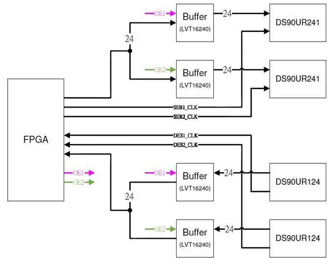
Due to insufficient FPGA IO, we currently want to use a set of outputs and inputs to drive more than two sets of DS90UR241/DS90UR124 respectively. The schematic diagram is as follows: