Part Number: LMH0397
Greetings,
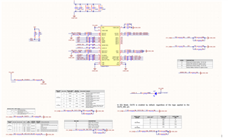
Please review this schematic and let us know your comments:

Best Regards, Gizem
This thread has been locked.
If you have a related question, please click the "Ask a related question" button in the top right corner. The newly created question will be automatically linked to this question.
Part Number: LMH0397
Greetings,
Please review this schematic and let us know your comments:

Best Regards, Gizem
Hi Gizem,
Thank you for sending. I reviewed with my team and concluded that the schematic does not have any critical issues. Here are a few comments.
Best,
Nick
Hi Nasser,
Thank you for your feedback. I will proceed to the layout stage, but I need an 8-layer stack up, can you help me? Do you have a stack up file for this kind of work or do you also use the LMH0397 material? Or what should I pay attention to when preparing the stack up? The recommended path thickness on the datasheet and eval board seems to be 10mil, can I draw a thinner path than this value?
Best Regards, Gizem
Hi Gizem,
Please contact your PCB manufacturer. The stack up should support a 75-ohm single ended trace and a 100-ohm differential trace. This is typically done with a layer 2 ground plane for the 100-ohm differential and a layer 3 ground plane for the single ended 75-ohm trace.
Do you have a stack up file for this kind of work or do you also use the LMH0397 material?
The recommended path thickness on the datasheet and eval board seems to be 10mil, can I draw a thinner path than this value?
Or what should I pay attention to when preparing the stack up?
Best,
Nick