This thread has been locked.

If you have a related question, please click the "Ask a related question" button in the top right corner. The newly created question will be automatically linked to this question.

HD3SS3212: Necessary to add bypass capacitor on TX line if two devices are daisy chained?

Part Number: HD3SS3212
Other Parts Discussed in Thread: TUSB522P

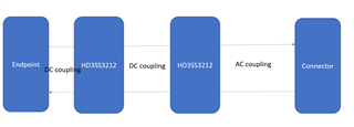
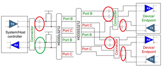
I have two HD3SS3212 are daisy chained and isolated from the surroundings using bypass capacitors on both RX and TX high speed lanes.
The two are biased to GND on the A0 and A1 ports.
The design is a USB3 5Gbit/s switch.

Is it necessary to isolate them using bypass capacitors in between and new bias resistors to maintain signal integrity?

We have problems with signal quality even though we have done the layout correctly (as we know it) and use a high quality pre-preg for high speed.

  • Hi,

    Can you please share your block diagram or schematic? I drew a rough block diagram on how to AC coupling two HD3SS3212 as shown below. The block diagram assumes the endpoint common mode voltage meets HD3SS3212 common mode voltage requirement. 

    What specific signal quality issue are you seeing? 

    Thanks

    David

  • I cannot show the exact details of our design but with some cutting from the documentation images I have added below a simplified schematic of what we have implemented. The PortC on the first HD3SS is going to other functionality to implement a multi port switch. The path shown below is an example of what is problematic for us.

    The bias resistors are connected to ground as it is stated that GND is a valid bias for the chips.
    I have tried to patch 1.5V bias with no change in behaviour.

    The problem we see is bad connnection on some USB3 hosts and OK connection on some. We have a PassMark USB3 looptest device to test for bit errors and throughput which indicates bad connection.,

    We have also had the opportunity to borrow a very competent instrument by Rohde & Schwartz which measured eye diagrams and impedance. Impedance seamed to be ok but the eye diagram were very much closed when using some devices and very narrow when using others.

    We have re-designed our board using small 0201 capacitors and other passivee components instead of 0402, we use pre-preg 7628 instead of 1080 and have now voided holes in the ground plane and all other relevant planes below the descrete component and connector pads along the entire path. I have no other idea of what can be wrong in the design. I'm trying to get hold of an instrument once again to measure the eye diagram after our latest design change which was the above change.
    I have put decoupling capacitors of 0.1 and 0.01uF under the chips.

    After the re-design of the layout I see slightly better bit error rate but far from acceptable.

    If there is a TI lab nearby Stockholm, Sweden, where I can have my eye-diagram measured again and perhaps also the impedance along the trace it would be of great help!

  • Hi,

    What is the value of the capacitor? The USB spec has the capacitance of min 75nF and max 265nF. So you want to make sure the total capacitance(capacitor at both side of MUX) stays within this range, otherwise you will have DC wander issue. 

    What is the targeted data rate for this design, 5Gbps or 10Gbps? You will have to take the insertion loss of the two HD3SS3212 into account along with the insertion loss of the PCB board trace, connector, via, etc. If you see the eye diagram being closed, then the insertion loss might be too big. Does the host controller have any de-emphasis control to provide compensation for the insertion loss? If not, any chance you can use a signal conditioner at the output of the 2nd HD3SS3212 and see if it helps compensating for the signal quality?

    We do not have a lab in Sweden that can support high speed USB eye diagram measurement. But I can support the eye diagram and TDR measurement in US if needed.

    Thanks

    David

  • The capacitors is 220nF. I have also tried 100nF and 470nF as the far end might have capacitors as well.
    I can add as a feedback that I did not find information of the probably best option to use 220nF caps in the case the host or device also has caps in the signal path. The datasheet says to use 100nF. I found this information first when reading the documentation of the development board of yours.

    The targetted data rate is 5GB/s.

    I cannot say if the host controller has a de-emphasis or if it is activated if so as I cannot get the datasheet of the chip from the manufacturer of the board or from the manufacturer of the chip mounted on the host board. What I see when analysing my design is that there are attenuation but the main factor for closing the eye diagram seam to be jitter in combination with the attenuation. I need better instrumentation to be able to measure the current attenuation.

    Thanks for the offer to measure in the US. I keep that in mind but for now I'm trying to get hold of a good enough instrument closer to Stockholm.

    I have been thinking about inserting some kind of re-driver or other signal conditioner but the space left on the device is limited so it would be difficult, but maybe not impossible. It would also first be good to understand what it is I'm trying to compensate for to get it right...

    We have now sent this updated design to production as it is usable but not really good in all aspects so I will have a better statistical outcome of the signal quality in a month or two.

  • Hello,

    Are there anymore questions that we can answer for you here?

    Thanks,

    Zach

  • If I understan you correctly my design is logically correct, i.e. it is not necessary to separate the two daisy chained chips DC wise and it is correct to have the bias resistors where they are situated in the diagram above I don't think I can get more help at the moment.

    If so you are free to close this issue as solved.
    If you can provide me with any more input that might help me create a better design in any way I'm open to suggestions.

    Regards
    Björn

  • Hello:

       Just one more question, do you have the same AC cap value on both TX and RX? RX AC cap value should be >300nf.

    Best

    Brian

  • I have the same value on all 8 positions. Do you have a reference for the need of using >300nF on RX?

    Also; can you define what you mean by "on RX"? Do you mean on both sides of the daisy chained chips on the SSRX diff pair or do you mean on the ingress side of both diff pairs of SSRX and SSTX?

    To be very clear you could edit the image above and draw a ring or arrow of the capacitors you think should use >300nF.

  • Hello:

                the green color on SSRX should be >300nf, the red color can be 220nf since there are two caps on SSTX host side.

    Did you try to remove bias and  AC caps close to host side?

    Regards'

    Brian

  • Thank you Brian

    Yes, I did try to remove the caps and bias resistors with no obvious improvement in bit error rate. As this was after I had access to the proper instrumentation I could not tell by the shape of the eye-diagram if a measurable improvement had been accomplished.

    My guess right now is that I have done what I can except for adding signal conditioning to compensate for the attenuation in my board. That is partly why I would like to get hold of the datasheet of the chip on the host board to see if it requires the device to bias the diff pair to something higher than GND or at all.

    I have given the producer of the USB3 host board feedback of my findings of the potential flaws in the design of there boards.

    Björn

  • Björn

    How long is the total trace length from the system controller to the connector? 

    For re-driver, I would propose using TUSB522P for this design.

    Thanks

    David

  • Our board has USB connectors on both ends and the total distance including the HD3SS is less than an inch or about 20mm. Then there is a 4-5 inch cable to the connector on the host board and another inch of traces on the host board. We are in the process of making custom made cables with better quality than the crappy ones you can buy of the shelf. They often have a bad wire termination when it comes to stripping the shield off with too long unshielded wires which results in a large impedance leap of over 125ohm as I have seen when measuring as well as cross talk. Whith correct termination shield stripping the impedance can be within spec or at least under 100 ohm.

    Thanks for the suggestion of the re-driver. I will keep that in mind for later if needed or for other designs similar to this. As the distance between the two USB connectors are quite short it will be difficult to squeeze in one or two re-drivers in this design but if we have to we will have to.

  • Hi,

    Since you have USB connector on both ends, you could connect the TUSB522P EVM (https://www.ti.com/tool/TUSB522PEVM) and see if it helps with the signal integrity. 

    Thanks

    David

  • Good idea!

    I consider this case closed as of now as I cannot get any more help and new boards are on the way.
    If necessay I open a new case here on the forum.

    Thanks for all the help!

    Björn