Part Number: DS90UB933-Q1
Hi,All!
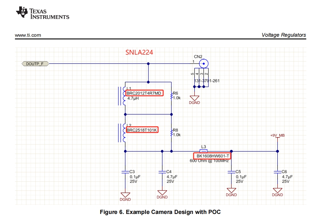
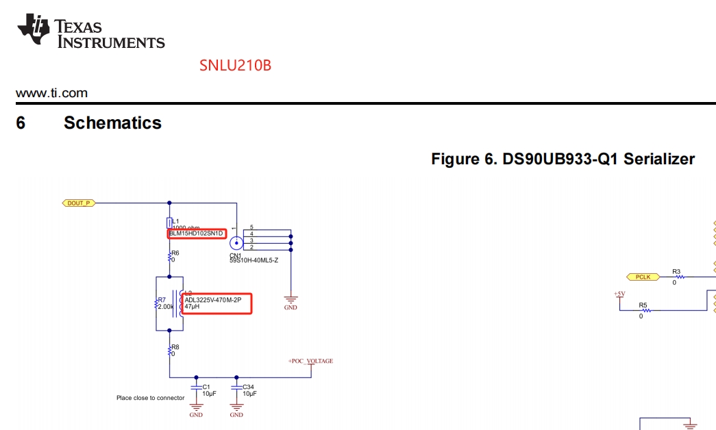
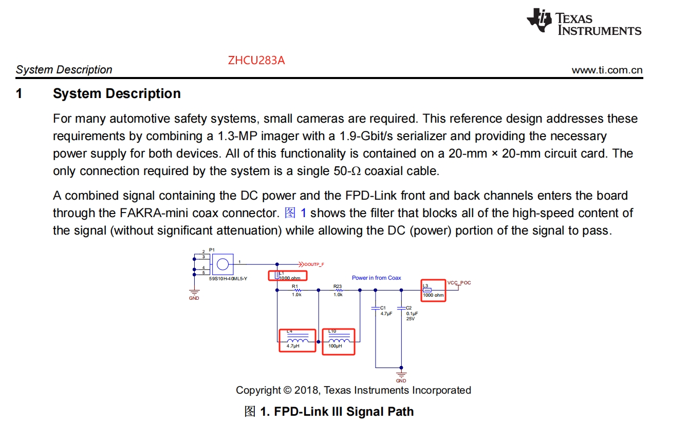
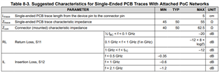
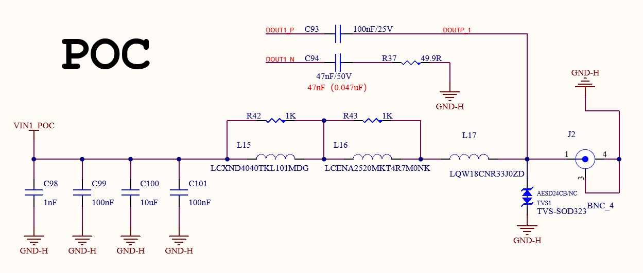
Using TI's device DS90UB933, please help check if the POC section is reasonable and see if there is any room for optimization.
1. The section of schematic.
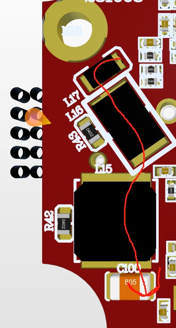
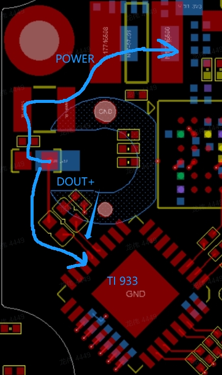
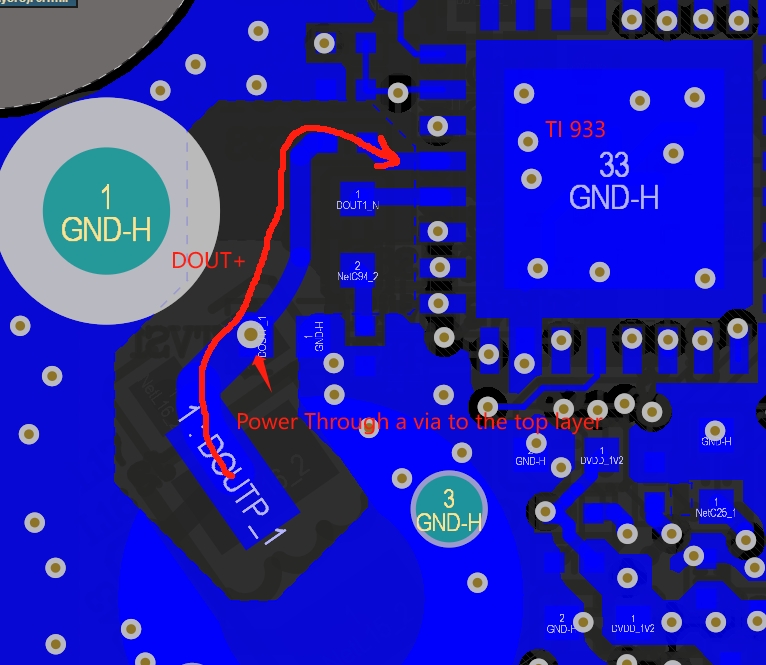
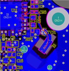
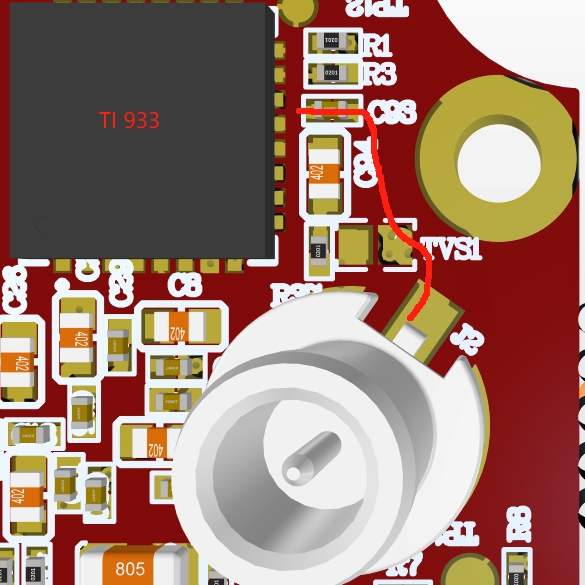
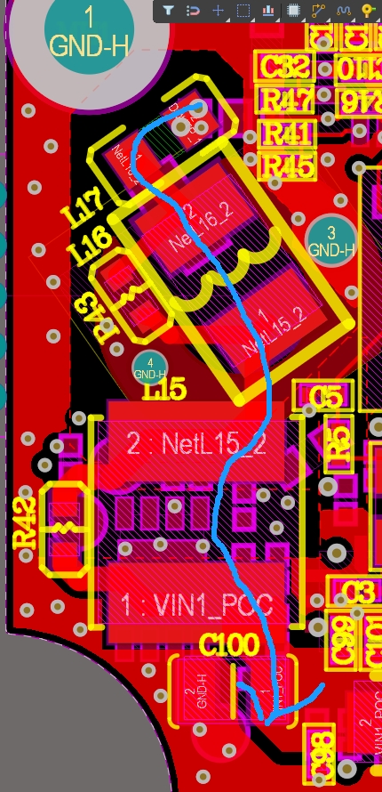
2.The section of PCB layout.
Bottom layer
3D Bottom layer
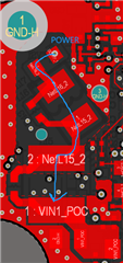
Top layer:
3D top layer
if there are any other needs, just let me know,looking forward to a reply,thank!