Part Number: DS280MB810
Other Parts Discussed in Thread: DS280DF810
Hi Team
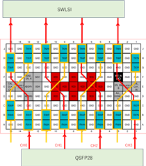
We are evaluating communication test (25G) with the setups by using QSFP28+DS280MB810+SWLSI.
Almost QSFP28s have no problems for communication test. In this case, register settings are below,
REG_0x03: 0xC0, REG_0x04: 0x91, REG_0x06: 0xC0, REG_0x0F: 0x00 for all channel. (CTLE Boost Settings are below)
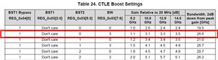
But one QSFP28 cannot be made error free. Changing CTLE Boost Settings from above becomes getting worse.
It is known that changing REG_0x0F: BG_SEL_IPP100[0/1], BG_SEL_IPH200_v0/1[0/1] will improve the situation. But it is not enough.
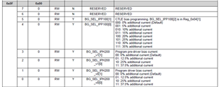
What is the pre-driver and driver in BG_SEL_IPH200? Boost1 and Boost2 ?
If we see improvement in these registers, what can we infer is wrong with this QSFP28 compared to other QSFP28s? Insufficient bandwidth?, insufficient amplitude?
Also, could you let us know if there are any other registers that could be improved?
How about REG_0x08: BG_SEL_IPTAT25?
Best Regards,
Mizobuchi