


Part Number: DS90UB941AS-Q1
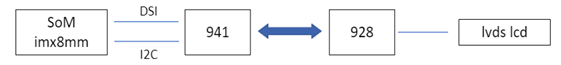
A simplified application diagram is as follows:
From the bringup guide, there are 4 steps. Step 1 to 3 are using PATGEN, step 4 do not use PATGEN, results are as follows:
- Step1 Enable PATGEN with Internal clock and internal timing which can be normally displayed.
- Step2 Enable PATGEN with External clock and Internal timing which can be normally displayed.
- Step3 Enable PATGEN with External clock and external timing which is not able to be shown.
- Step4 Disable PATGEN with External clock and external timing which is not able to be shown.
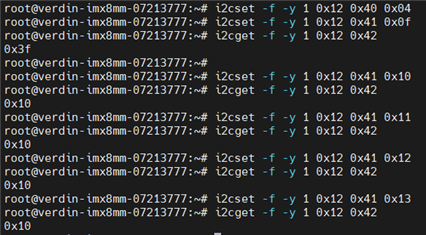
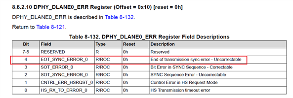
For step4, Multiple attempts were made using the SoC's DSI data and clock and the screen still does not turn on. The DSI output is configured for video mode, burst mode, continuous clock mode. Through oscilloscope, it can be seen that the DSI can output normally. However, after the register configuration is performed, the screen still does not work. Checked DPHY related registers 0xF,0x10,0x11,0x12,0x13,0x14,0x15, status register values of all four data lane are 0x14 = 0001 0000, where bit4 are indicated with errors:
The register configuration for step 4 is as follows:
#!/bin/bash

# 800x480p60, Dual Link FPD III
# PCLK = 33.264MHz
# DSI clock = 99.792MHz
# DSI Lane Speed = 199.584Mbps/lane
# 4 Lanes DSI
# DSI input port 0
# DSI clock and DSI data
# use i2c-tools to debug

set -e

I2C_BUS_NUMBER=1
UB941AS_ADDR=0x12
UB928_ADDR=0x2c

# Disable DSI
i2cset -y -f -r $I2C_BUS_NUMBER $UB941AS_ADDR 0x01 0x08

# Select FPD-Link III Port 0
i2cset -y -f -r $I2C_BUS_NUMBER $UB941AS_ADDR 0x1e 0x01

# Enable I2C_PASSTHROUGH
i2cset -y -f -r $I2C_BUS_NUMBER $UB941AS_ADDR 0x03 0x9a

# Force select port 0
i2cset -y -f -r $I2C_BUS_NUMBER $UB941AS_ADDR 0x5b 0x21

# Select DSI Port 0 digital registers
i2cset -y -f -r $I2C_BUS_NUMBER $UB941AS_ADDR 0x40 0x04
# Select DSI_CONFIG_0 register
i2cset -y -f -r $I2C_BUS_NUMBER $UB941AS_ADDR 0x41 0x20
# Set DSI_SYNC_PULSES = 0
i2cset -y -f -r $I2C_BUS_NUMBER $UB941AS_ADDR 0x42 0x6f

# Select DSI_CONFIG_1 register
i2cset -y -f -r $I2C_BUS_NUMBER $UB941AS_ADDR 0x41 0x21
# Set DSI_VS_POLARITY=DSI_HS_POLARITY=1
i2cset -y -f -r $I2C_BUS_NUMBER $UB941AS_ADDR 0x42 0x60

# Set DSI_CONTINUOUS_CLOCK, single DSI, 4 lanes, DSI Port 0 input
i2cset -y -f -r $I2C_BUS_NUMBER $UB941AS_ADDR 0x4f 0x8c

# DSI_HSW_CFG_HI
i2cset -y -f -r $I2C_BUS_NUMBER $UB941AS_ADDR 0x41 0x30
i2cset -y -f -r $I2C_BUS_NUMBER $UB941AS_ADDR 0x42 0x00
# DSI_HSW_CFG_LO  hsync-len = 48
i2cset -y -f -r $I2C_BUS_NUMBER $UB941AS_ADDR 0x41 0x31
i2cset -y -f -r $I2C_BUS_NUMBER $UB941AS_ADDR 0x42 0x30
# DSI_VSW_CFG_HI
i2cset -y -f -r $I2C_BUS_NUMBER $UB941AS_ADDR 0x41 0x32
i2cset -y -f -r $I2C_BUS_NUMBER $UB941AS_ADDR 0x42 0x00
# DSI_VSW_CFG_LO  vsync-len = 1
i2cset -y -f -r $I2C_BUS_NUMBER $UB941AS_ADDR 0x41 0x33
i2cset -y -f -r $I2C_BUS_NUMBER $UB941AS_ADDR 0x42 0x01

# TSKIP_CNT set DSI/D-PHY port0  TSKIP_CNT = round(65x0.099792-5) =1  --->   << 1  = 0x02
i2cset -y -f -r $I2C_BUS_NUMBER $UB941AS_ADDR 0x40 0x04
# TSKIP_CNT set indirect addr (reg DPHY_SKIP_TIMING)
i2cset -y -f -r $I2C_BUS_NUMBER $UB941AS_ADDR 0x41 0x05
# TSKIP_CNT set reg DPHY_SKIP_TIMING value
i2cset -y -f -r $I2C_BUS_NUMBER $UB941AS_ADDR 0x42 0x02

# Initialize DSI clock settings (From Section 10.2 of datasheet)
i2cset -y -f $I2C_BUS_NUMBER $UB941AS_ADDR 0x40 0x10
i2cset -y -f $I2C_BUS_NUMBER $UB941AS_ADDR 0x41 0x86
i2cset -y -f $I2C_BUS_NUMBER $UB941AS_ADDR 0x42 0x0A
i2cset -y -f $I2C_BUS_NUMBER $UB941AS_ADDR 0x41 0x94
i2cset -y -f $I2C_BUS_NUMBER $UB941AS_ADDR 0x42 0x0A

# Enable DSI
i2cset -y -f -r $I2C_BUS_NUMBER $UB941AS_ADDR 0x01 0x00
The register configuration for step 3 is as follows:
#!/bin/bash

# 800x480p60, Dual Link FPD III
# PCLK = 33.264MHz
# DSI clock = 99.792MHz
# DSI Lane Speed = 199.584Mbps/lane
# 4 Lanes DSI
# DSI input port 0
# Pattern Generator Mode
# dsi clock and dsi timing
# use i2c-tools to debug

set -e

I2C_BUS_NUMBER=1
UB941AS_ADDR=0x12
UB928_ADDR=0x2c

# Disable DSI
i2cset -y -f -r $I2C_BUS_NUMBER $UB941AS_ADDR 0x01 0x08

# Select FPD-Link III Port 0
i2cset -y -f -r $I2C_BUS_NUMBER $UB941AS_ADDR 0x1e 0x01

# Enable I2C_PASSTHROUGH
i2cset -y -f -r $I2C_BUS_NUMBER $UB941AS_ADDR 0x03 0x9a

# Force select port 0
i2cset -y -f -r $I2C_BUS_NUMBER $UB941AS_ADDR 0x5b 0x21

# Select DSI Port 0 digital registers
i2cset -y -f -r $I2C_BUS_NUMBER $UB941AS_ADDR 0x40 0x04
# Select DSI_CONFIG_0 register
i2cset -y -f -r $I2C_BUS_NUMBER $UB941AS_ADDR 0x41 0x20
# Set DSI_SYNC_PULSES = 0
i2cset -y -f -r $I2C_BUS_NUMBER $UB941AS_ADDR 0x42 0x6f

# Select DSI_CONFIG_1 register
i2cset -y -f -r $I2C_BUS_NUMBER $UB941AS_ADDR 0x41 0x21
# Set DSI_VS_POLARITY=DSI_HS_POLARITY=1
i2cset -y -f -r $I2C_BUS_NUMBER $UB941AS_ADDR 0x42 0x60

# Set DSI_CONTINUOUS_CLOCK, single DSI, 4 lanes, DSI Port 0 input
i2cset -y -f -r $I2C_BUS_NUMBER $UB941AS_ADDR 0x4f 0x8c

# DSI_HSW_CFG_HI
i2cset -y -f -r $I2C_BUS_NUMBER $UB941AS_ADDR 0x41 0x30
i2cset -y -f -r $I2C_BUS_NUMBER $UB941AS_ADDR 0x42 0x00
# DSI_HSW_CFG_LO  hsync-len = 48
i2cset -y -f -r $I2C_BUS_NUMBER $UB941AS_ADDR 0x41 0x31
i2cset -y -f -r $I2C_BUS_NUMBER $UB941AS_ADDR 0x42 0x30
# DSI_VSW_CFG_HI
i2cset -y -f -r $I2C_BUS_NUMBER $UB941AS_ADDR 0x41 0x32
i2cset -y -f -r $I2C_BUS_NUMBER $UB941AS_ADDR 0x42 0x00
# DSI_VSW_CFG_LO  vsync-len = 1
i2cset -y -f -r $I2C_BUS_NUMBER $UB941AS_ADDR 0x41 0x33
i2cset -y -f -r $I2C_BUS_NUMBER $UB941AS_ADDR 0x42 0x01

# TSKIP_CNT set DSI/D-PHY port0  TSKIP_CNT = round(65x0.099792-5) =1  --->   << 1  = 0x02
i2cset -y -f -r $I2C_BUS_NUMBER $UB941AS_ADDR 0x40 0x04
# TSKIP_CNT set indirect addr (reg DPHY_SKIP_TIMING)
i2cset -y -f -r $I2C_BUS_NUMBER $UB941AS_ADDR 0x41 0x05
# TSKIP_CNT set reg DPHY_SKIP_TIMING value
i2cset -y -f -r $I2C_BUS_NUMBER $UB941AS_ADDR 0x42 0x02

# Initialize DSI clock settings (From Section 10.2 of datasheet)
i2cset -y -f $I2C_BUS_NUMBER $UB941AS_ADDR 0x40 0x10
i2cset -y -f $I2C_BUS_NUMBER $UB941AS_ADDR 0x41 0x86
i2cset -y -f $I2C_BUS_NUMBER $UB941AS_ADDR 0x42 0x0A
i2cset -y -f $I2C_BUS_NUMBER $UB941AS_ADDR 0x41 0x94
i2cset -y -f $I2C_BUS_NUMBER $UB941AS_ADDR 0x42 0x0A

# Enable DSI
i2cset -y -f -r $I2C_BUS_NUMBER $UB941AS_ADDR 0x01 0x00

# 1. Set Pixel Clock and Active Frame Size
# pixe clock = 33.264MHz  divider = 200/33.264 ≈ 6
# hactive = 800 vactive = 480
#

i2cset -y -f -r $I2C_BUS_NUMBER $UB941AS_ADDR 0x66 0x03
i2cset -y -f -r $I2C_BUS_NUMBER $UB941AS_ADDR 0x67 0x06

i2cset -y -f -r $I2C_BUS_NUMBER $UB941AS_ADDR 0x66 0x07
i2cset -y -f -r $I2C_BUS_NUMBER $UB941AS_ADDR 0x67 0x20

i2cset -y -f -r $I2C_BUS_NUMBER $UB941AS_ADDR 0x66 0x08
i2cset -y -f -r $I2C_BUS_NUMBER $UB941AS_ADDR 0x67 0x03

i2cset -y -f -r $I2C_BUS_NUMBER $UB941AS_ADDR 0x66 0x09
i2cset -y -f -r $I2C_BUS_NUMBER $UB941AS_ADDR 0x67 0x1E

# 2. Set Total Frame Size
# Total H Width = 40(hback porch) + 800(hactive) + 40(hfront porch) + 48(hsync len)
#		= 928 = 0011 1010 0000
# Total V Width = 31(vback porch) + 480(vactive) + 13(vfront porch) + 1(vsync len)
#               = 525 = 0010 0000 1101
#
i2cset -y -f -r $I2C_BUS_NUMBER $UB941AS_ADDR 0x66 0x04
i2cset -y -f -r $I2C_BUS_NUMBER $UB941AS_ADDR 0x67 0xA0

i2cset -y -f -r $I2C_BUS_NUMBER $UB941AS_ADDR 0x66 0x05
i2cset -y -f -r $I2C_BUS_NUMBER $UB941AS_ADDR 0x67 0xD3

i2cset -y -f -r $I2C_BUS_NUMBER $UB941AS_ADDR 0x66 0x06
i2cset -y -f -r $I2C_BUS_NUMBER $UB941AS_ADDR 0x67 0x20

# 3. Set Back Porch
# H Back Porch = 40 = 0010 1000
# V Back Porch = 31 = 0001 1111
i2cset -y -f -r $I2C_BUS_NUMBER $UB941AS_ADDR 0x66 0x0C
i2cset -y -f -r $I2C_BUS_NUMBER $UB941AS_ADDR 0x67 0x28

i2cset -y -f -r $I2C_BUS_NUMBER $UB941AS_ADDR 0x66 0x0D
i2cset -y -f -r $I2C_BUS_NUMBER $UB941AS_ADDR 0x67 0x1F

# 4. Set Sync Widths
# H Sync Width = 48 = 0011 0000
# V Sync Width = 1  = 0000 0001
i2cset -y -f -r $I2C_BUS_NUMBER $UB941AS_ADDR 0x66 0x0A
i2cset -y -f -r $I2C_BUS_NUMBER $UB941AS_ADDR 0x67 0x30

i2cset -y -f -r $I2C_BUS_NUMBER $UB941AS_ADDR 0x66 0x0B
i2cset -y -f -r $I2C_BUS_NUMBER $UB941AS_ADDR 0x67 0x01

# 5. Set Sync Polarities
i2cset -y -f -r $I2C_BUS_NUMBER $UB941AS_ADDR 0x66 0x0E
i2cset -y -f -r $I2C_BUS_NUMBER $UB941AS_ADDR 0x67 0x03

# 6. Enable Pattern Generation
# reverse color
i2cset -y -f -r $I2C_BUS_NUMBER $UB941AS_ADDR 0x65 0x02

# set color and enable Pattern Generator
i2cset -y -f -r $I2C_BUS_NUMBER $UB941AS_ADDR 0x64 0xd5
For step3, After configuration, DSI_VC_DTYPE reads as 0x3e.
And use an oscilloscope to capture the waveform of lane 0 as follows:
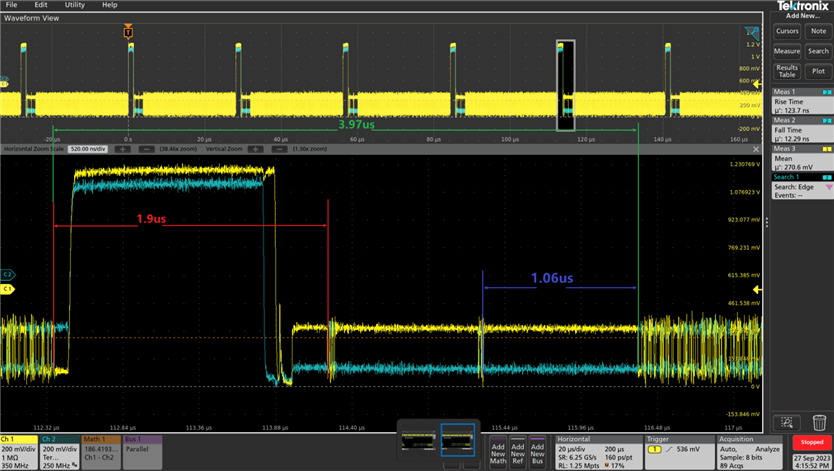
1) Dose this error indicating the SoC's DSI output is not configured correctly? Or what else error?
