Other Parts Discussed in Thread: SN65LVDS105,
I have a design where I plan on generating a reference clock using a 64MHz CMOS oscillator, which I then bring to a SN65LVDS105 (CMOS to 4x LVDS). Three of the SN65LVDS105's outputs then go to three SN65LVDS116, to create a total of 48 LVDS clocks. These 48 LVDS clocks go to 48 PCIe-type of connectors (so board-to-board, no cabling), which may or not be inserted.
I want to make sure I properly terminate my receivers, but it's unclear from the datasheet what external components are suggested. I can't even figure out if the SN65LVDS116 receiver has internal termination or not (Figure 12 seems to suggest that it's internal, but the "equivalent input and output schematic diagrams" seems to suggest that it's not).
Could you please provide some guidance as to what should be on my LVDS lines between the SN65LVDS105 and my SN65LVDS116, as well as between the SN65LVDS116 and the receiver on the daughter board?
- AC coupling capacitors? If so, what's the optimal location for these (near the driver, near the receiver, near connector on the motherboard, near the connector on the daughter board)?
- DC biasing resistors?
- Common mode choke (e.g. DLW21SZ900HQ2L or similar)? Where's the optimal place to put this at?
- Series resistors at driver?
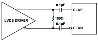
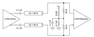
- Termination scheme? E.g. just 100ohm between, or 50 and 50 with cap to GND?
I've seen several app notes that show the use of different schemes (such as SLAA840), but I'd like to know which setup would be recommended for this application.
Note that the daughter board's receiver needs an external termination resistor and 100nF capacitors:


