This thread has been locked.

If you have a related question, please click the "Ask a related question" button in the top right corner. The newly created question will be automatically linked to this question.

TCA9517A: interval time

Part Number: TCA9517A
Other Parts Discussed in Thread: TCA9517

Hi team,

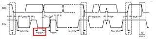
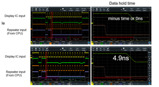
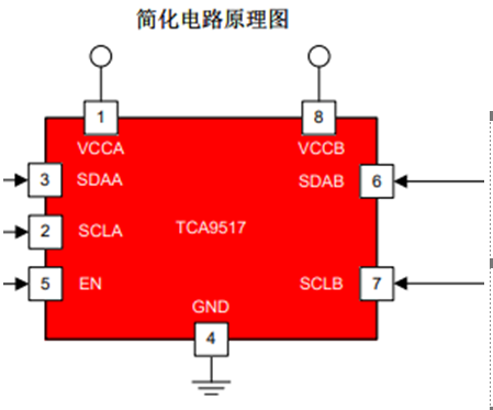
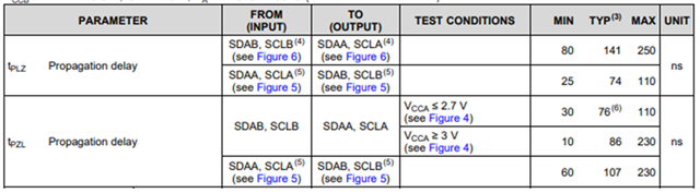
The datasheet shows the delay time of A to B or B to A, but if the interval between SDAA and SCLA during input is 5ns, can the interval between SDAB and SCLB at the output end also be maintained at 5ns?

Thanks

Lillian

  • Hi Lillian,

    You're asking about the channel skew between SCL and SDA? We don't spec this in our datasheet and don't have data on this. Is there a specific reason you need this? This device was designed specifically for I2C communication which doesn't care about the channel skew between SDA and SCL because there is so much time/margin for this in I2C that it doesn't really matter. Is your customer not using this device for I2C purposes?

    -Bobby

  • Hi Bobby,

    Because we have found that some I2C ACK failures are due to data hold time not enough to meet the I2C requirements.

    You can see below waveform , the Thd;DAT from CPU side is about 5ns . But after two repeater IC , the Thd;DAT become to minus or 0ns .

    But the other product is 4.9ns, so is the channel skew between SCL and SDA controllable by the chip or random?

    Thanks

    Lillian

  • Hi Lillian,

    Thanks for the background on this.

    You can see below waveform

    Is this with 2 separate boards (top waveform is board 1 and bottom waveform board 2) or did you use 1 board but replace the TCA9517? A portion of this may also be related to the CPU generating the signals as well having a different skew. With two different boards, it would make it hard to tell if 9517 or the CPU generated the most skew difference.

    But the other product is 4.9ns, so is the channel skew between SCL and SDA controllable by the chip or random?

    We don't test for the skew times between channels as this normally doesn't matter for I2C (explanation below). 

    The data hold time is a system level specification for the I2C Bus. From a I2C device state machine perspective, the data hold times shouldn't cause problems with data sampling or missed ACKs because the data is supposed to be sampled on rising clock edges, not falling clock edges (in my opinion data set up time is a more important parameter for this reason than data hold times). If a device is failing or getting improper data because of this, it means the device itself is trying to sample data on the falling clock edges which gives very little margin for the time for data to transition and be ready for sampling.  

    --------------

    A workaround:

    From a system level, you can help provide more margin by changing the RC constant on the data signal. Since the timing for hold time is based on the falling edge, the R in the RC constant is the pull down FET  of the device generating the data signal. You can put a series resistor infront of the device generating the clock signal to make the R larger thus slowing down the fall time or you can increase the capacitance on the data line to make the RC larger (will affect the rise time as well though). You could also do both. 

    Alternatively, you could also have another TCA9517 where you route the SDA line through SDAB into SDAA into SCLA into SCLB and have the clock signal NOT go through the buffer. This would force the SDA signal to go through 2x prop delays of a TCA9517 and the SCL signal would have much more set up time margin. 

    -Bobby