This thread has been locked.

If you have a related question, please click the "Ask a related question" button in the top right corner. The newly created question will be automatically linked to this question.

DS90UB941AS-Q1: Sync pulse problem after deserialization

Part Number: DS90UB941AS-Q1
Other Parts Discussed in Thread: ALP

Hi,

I'm using a DS90UB941AS-Q1 sererializer combined with 2 DS90UB948 deserializer.

In this example the serializer is configured in "independent mode" and there's 1 JEIDA/HDMI adapter appended on the deserializer
on port0.

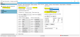
DSI input is configured to use Non-Burst Mode with Sync Pulses but I have a problem on the OLDI signal after the deserializtion.

Problem is the  VSync pulse signal is always low and HSync is moving high. They look like this:
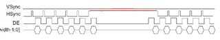
  

Expected signals:


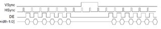
Inizializatoin sequence:

# initialize port 0 registers on serializer
18:22:52[936351250] ==> i2cset -y 5a820000.i2c 0x0c 0x1e 0x01
18:22:52[948901000] ==> i2cset -y 5a820000.i2c 0x0c 0x03 0xda

# overide the deserializer address to 0x20 on port 0
18:22:52[987897875] ==> i2cset -y 5a820000.i2c 0x2c 0x00 65

# initialize port 1 registers on serializer
18:22:52[998290750] ==> i2cset -y 5a820000.i2c 0x0c 0x1e 0x02
18:22:53[011161000] ==> i2cset -y 5a820000.i2c 0x0c 0x03 0xda

# overide the deserializer address to 0x30 on port 1
18:22:53[062667375] ==> i2cset -y 5a820000.i2c 0x2c 0x00 97

# set aliases on port 1
18:22:53[073215000] ==> i2cset -y 5a820000.i2c 0x0c 0x1e 0x1
18:22:53[086556250] ==> i2cset -y 5a820000.i2c 0x0c 0x07 148
18:22:53[098336500] ==> i2cset -y 5a820000.i2c 0x0c 0x08 74
18:22:53[111181625] ==> i2cset -y 5a820000.i2c 0x0c 0x70 128
18:22:53[124117250] ==> i2cset -y 5a820000.i2c 0x0c 0x77 66
18:22:53[137289250] ==> i2cset -y 5a820000.i2c 0x0c 0x71 48
18:22:53[149469000] ==> i2cset -y 5a820000.i2c 0x0c 0x78 68

# set aliases on port 2
18:22:53[162997500] ==> i2cset -y 5a820000.i2c 0x0c 0x1e 0x2
18:22:53[175168250] ==> i2cset -y 5a820000.i2c 0x0c 0x07 148
18:22:53[190164000] ==> i2cset -y 5a820000.i2c 0x0c 0x08 106
18:22:53[201068500] ==> i2cset -y 5a820000.i2c 0x0c 0x70 128
18:22:53[215402000] ==> i2cset -y 5a820000.i2c 0x0c 0x77 98
18:22:53[226420125] ==> i2cset -y 5a820000.i2c 0x0c 0x71 48

# finish initialization and start DSI
18:22:53[240726875] ==> i2cset -y 5a820000.i2c 0x0c 0x78 100
18:22:53[252157125] ==> i2cset -y 5a820000.i2c 0x0c 0x5b 0x05
18:22:53[266714500] ==> i2cset -y 5a820000.i2c 0x0c 0x12 0x02
18:22:53[277798875] ==> i2cset -y 5a820000.i2c 0x0c 0x1e 0x04
18:22:53[292367750] ==> i2cset -y 5a820000.i2c 0x0c 0x01 0x00

# initialize deserializer on port 0
18:22:53[315180125] ==> i2cset -y 5a820000.i2c 0x20 0x01 0x02
18:22:53[328120500] ==> i2cset -y 5a820000.i2c 0x20 0x05 0x9e
18:22:53[341034875] ==> i2cset -y 5a820000.i2c 0x20 0x26 0x32
18:22:53[353973750] ==> i2cset -y 5a820000.i2c 0x20 0x27 0x32
18:22:53[366440375] ==> i2cset -y 5a820000.i2c 0x20 0x49 0x02

  • Hi Matteo,

    Are you sure the input signal is not getting corrupted from the source ? How are you verifying that?

    So you have 941AS setup in independent mode and you have port0 Vsync issue , but port1 is working as expected with no issues? 

    Have you tried isolating the issue further by running internal patgen from 941AS to see if that shows the same Vsync issue? 

    Regards,
    Fadi A.

  • Are you sure the input signal is not getting corrupted from the source ? How are you verifying that?

    Unfortunately I can't get the output signal directly. I don't have the test points and I'm not able to decode the DSI signal.

    Is there a way to do this from the serializer? I mean, is possible to use some registers to understand if the DSI signnal from input is like expected?

  • Have you tried isolating the issue further by running internal patgen from 941AS to see if that shows the same Vsync issue? 

    Yes. Activating Pathgen the adaptor works properly. No Vsync issue. And all pattern are displayed.

  • Hi Matteo,

    I will review and get back to you tomorrow. Thanks. 

    Regards,
    Fadi A.

  • So you have 941AS setup in independent mode and you have port0 Vsync issue , but port1 is working as expected with no issues? 

    Port1 show exactly the same behavior.

  • Hey Matteo

    Yes. Activating Pathgen the adaptor works properly. No Vsync issue. And all pattern are displayed.

    Since patgen works properly from 941AS the issue is most likely coming from the video source. Next step, you need to check whether the issue is timing or CLK issue. We have a few modes that you could run for additional debug. 941AS supports multiple modes:

    1- Internal - everything will be internally generated; HS, VS, DE, CLK and Video (if no issue is observed then the issue is likely coming from the video source)

    2- Internal w/ext clk is HS, VS, DE and Video are generated internally but using External PCLK (if you see an issue in this mode, this point to an external CLK issue from the source) 

    3-  External is HS, VS, DE and CLK are generated externally (if you see an issue in this mode, this point to an external CLK/timing issue from the source) 

    If you have ALP you could do this type of testing from the user-interface and select different timing sources with different resolutions and patterns. 

    If you don't have ALP ... Here is an example script of running patgen with internal timing for 854x480 res and PCLK:33.3 Mhz .. you could program your timing and CLK into it or give me your timing and I could generate a script for you. But looking at the example script you see that register 0x65 is the one where you could switch between the timing modes.

    Example: board.WriteI2C(Ser_addr,0x65,0x04) #using internal timing and internal clock

    #This script is generated for an STP system for the following timing 
    # Resolution: 854 480
    #TH = 1000 , TV = 525
    # HFP HBP HSYNC:68 72 6
    # VFP  VBP VSYNC:35 9 1
    # PCLK:33.3 Mhz
    
    
    import time
    Ser_addr = 0x18
    
    time.sleep(0.5)
    board.WriteI2C(Ser_addr,0x01,0x08) # Reset
    board.WriteI2C(Ser_addr,0x01,0x02) # Reset
    
    board.WriteI2C(Ser_addr,0x3,0xDA) #Passthrough I2C
    
    time.sleep(0.5)
    board.WriteI2C(Ser_addr,0x5B,0x00) #Auto-detect 
    
    board.WriteI2C(Ser_addr,0x1E,0x01) #Select FPD-Link III Port 0
    board.WriteI2C(Ser_addr,0x66,0x1A)
    board.WriteI2C(Ser_addr,0x67,0x01) #M=1
    board.WriteI2C(Ser_addr,0x66,0x03)
    board.WriteI2C(Ser_addr,0x67,0x06) #N=6
    
    board.WriteI2C(Ser_addr,0x66,0x04)
    board.WriteI2C(Ser_addr,0x67,0xE8) #least 8 bit of Total Horizontal frame size
    board.WriteI2C(Ser_addr,0x66,0x05)
    board.WriteI2C(Ser_addr,0x67,0xD3) #Least 4 bit TV + Most 4 bit TH
    board.WriteI2C(Ser_addr,0x66,0x06)
    board.WriteI2C(Ser_addr,0x67,0x20) #Most 8 bit of Total Vertical frame size
    
    board.WriteI2C(Ser_addr,0x66,0x07)
    board.WriteI2C(Ser_addr,0x67,0x56) #least 8 bit of active Horizontal frame size
    board.WriteI2C(Ser_addr,0x66,0x08)
    board.WriteI2C(Ser_addr,0x67,0x03) #Least 4 bit AV + Most 4 bit AH
    board.WriteI2C(Ser_addr,0x66,0x09)
    board.WriteI2C(Ser_addr,0x67,0x1E) #Most 8 bit of active Vertical frame size
    
    board.WriteI2C(Ser_addr,0x66,0x0A)
    board.WriteI2C(Ser_addr,0x67,0x06) #Horizontal Sync Width
    board.WriteI2C(Ser_addr,0x66,0x0B)
    board.WriteI2C(Ser_addr,0x67,0x01) #Vertical Sync Width
    board.WriteI2C(Ser_addr,0x66,0x0C)
    board.WriteI2C(Ser_addr,0x67,0x48) #Horizontal back porch
    board.WriteI2C(Ser_addr,0x66,0x0D)
    board.WriteI2C(Ser_addr,0x67,0x09) #Vertical back porch
    board.WriteI2C(Ser_addr,0x65,0x04) #using internal timing and internal clock
    board.WriteI2C(Ser_addr,0x64,0x15) #enable PG/color bars
    
    
    board.WriteI2C(Ser_addr,0x1E,0x01) #Select FPD-Link III Port 0
    board.WriteI2C(Ser_addr,0x07,0x58) #0x07,0x58
    board.WriteI2C(Ser_addr,0x08,0x5C) #0x08,0x5c
    board.WriteI2C(Ser_addr,0x03,0x9A) #0x03,0x9A Enable I2C_PASSTHROUGH, FPD-Link III Port 0
    
    board.WriteI2C(Ser_addr,0x01,0x00) #Release DSI

    Is there a way to do this from the serializer? I mean, is possible to use some registers to understand if the DSI signnal from input is like expected?

    Yes we could check the DSI registers to see if there any DSI errors, etc. Once you run this script it will generate an excel file within the same directory the script is saved to and will dump main page and DSI page registers for both ports. 

    import time
    
    devAddr = 0x18
    device = "941AS"
    
    dateTime = time.strftime("%Y%m%d-%H%M%S")
    csv_name = 'PageDump' + str(device) +'_'+  dateTime  + '.csv'
    f1=open(csv_name, 'w+')
    
    
    # MainPage Dump for 941AS
    f1.write("MainPage\n")
    f1.write("Register Address, Register Value\n")
    for x in range(0,256):
    		val = hex(x)
    		f1.write(str(val)+",")
    		val = hex(board.ReadI2C(devAddr, x))
    		f1.write(str(val) + ",\n")
    f1.write("\r\n")
    print "Main Page Done"
    
    
    # DSI Port 0 Page Dump
    f1.write("DSI Port 0\n")
    f1.write("Register Address, Register Value\n")
    board.WriteI2C(devAddr,0x40,0x5)
    for x in range(0,59):
    	val = hex(x)
    	f1.write(str(val)+",")
    	board.WriteI2C(devAddr, 0x41, x)
    	val=board.ReadI2C(devAddr,0x42)
    	f1.write(str(hex(val)) + ",\n")
    print "DSI Port 0 Complete"
    f1.write("\r\n")
    
    # DSI Port 1 Page Dump
    f1.write("DSI Port 1\n")
    f1.write("Register Address, Register Value\n")
    board.WriteI2C(devAddr,0x40,0x8)
    for x in range(0,59):
    	val = hex(x)
    	f1.write(str(val)+",")
    	board.WriteI2C(devAddr, 0x41, x)
    	val=board.ReadI2C(devAddr,0x42)
    	f1.write(str(hex(val)) + ",\n")
    print "DSI Port 1 Complete"
    f1.write("\r\n")


    f1.flush()
    f1.close()
    print "Complete"
    

    Regards,
    Fadi A.

  • 1- Internal - everything will be internally generated; HS, VS, DE, CLK and Video (if no issue is observed then the issue is likely coming from the video source)

    2- Internal w/ext clk is HS, VS, DE and Video are generated internally but using External PCLK (if you see an issue in this mode, this point to an external CLK issue from the source) 

    3-  External is HS, VS, DE and CLK are generated externally (if you see an issue in this mode, this point to an external CLK/timing issue from the source) 

    Unfortunately I don't have the possibility to use ALP but importing and adapting your code in my init script I could check these points:
    1 - internal: clock and signals are correctly generated. colors bars are displayed OK.
    2 - external clock and internal signals: I change the value of the reg[0x65] from 0x04 to 0x0C and still works properly.
    3 - external clock and external signals: I change the value of the reg[0x65] from 0x04 to 0x08 and in this configuration problem occurs

    In detail, when the error occurs the VS and HS puleses seems blocked in a strage behaviour.
    From my prospective the DSI signal generated should only use "NO burst with sync pulses".

    In attachment a picture of the registers when the error occurs.
    Is possible to understand from these dumps if my DSI controller is initialized correctly or if there is something activated i.e
    not compatible with the DS90UB941AS-Q1?


    MainPage
    Register Address, Register Value
    0x0,0x18,
    0x1,0x00,
    0x2,0x00,
    0x3,0xda,
    0x4,0x00,
    0x5,0x00,
    0x6,0x40,
    0x7,0x00,
    0x8,0x00,
    0x9,0x01,
    0xa,0x12,
    0xb,0x00,
    0xc,0x67,
    0xd,0x30,
    0xe,0x00,
    0xf,0x00,
    0x10,0x00,
    0x11,0x00,
    0x12,0x02,
    0x13,0x9b,
    0x14,0x00,
    0x15,0x00,
    0x16,0xfe,
    0x17,0x1e,
    0x18,0x7f,
    0x19,0x7f,
    0x1a,0x01,
    0x1b,0x00,
    0x1c,0x01,
    0x1d,0x00,
    0x1e,0x04,
    0x1f,0x00,
    0x20,0x0b,
    0x21,0x00,
    0x22,0x25,
    0x23,0x00,
    0x24,0x00,
    0x25,0x00,
    0x26,0x00,
    0x27,0x00,
    0x28,0x01,
    0x29,0x20,
    0x2a,0x20,
    0x2b,0xa0,
    0x2c,0x00,
    0x2d,0x00,
    0x2e,0xa5,
    0x2f,0x5a,
    0x30,0x00,
    0x31,0x09,
    0x32,0x00,
    0x33,0x05,
    0x34,0x0c,
    0x35,0x00,
    0x36,0x00,
    0x37,0x00,
    0x38,0x00,
    0x39,0x00,
    0x3a,0x00,
    0x3b,0x00,
    0x3c,0x00,
    0x3d,0x00,
    0x3e,0x81,
    0x3f,0x02,
    0x40,0x10,
    0x41,0x94,
    0x42,0x00,
    0x43,0x00,
    0x44,0x00,
    0x45,0x00,
    0x46,0x00,
    0x47,0x00,
    0x48,0x00,
    0x49,0x00,
    0x4a,0x00,
    0x4b,0x00,
    0x4c,0x00,
    0x4d,0x00,
    0x4e,0x00,
    0x4f,0x8c,
    0x50,0x16,
    0x51,0x00,
    0x52,0x00,
    0x53,0x00,
    0x54,0x02,
    0x55,0x00,
    0x56,0x00,
    0x57,0x02,
    0x58,0x00,
    0x59,0x00,
    0x5a,0xd9,
    0x5b,0x05,
    0x5c,0x07,
    0x5d,0x06,
    0x5e,0x44,
    0x5f,0x41,
    0x60,0x22,
    0x61,0x02,
    0x62,0x00,
    0x63,0x00,
    0x64,0x10,
    0x65,0x00,
    0x66,0x00,
    0x67,0x00,
    0x68,0x00,
    0x69,0x00,
    0x6a,0x00,
    0x6b,0x00,
    0x6c,0x00,
    0x6d,0x00,
    0x6e,0x20,
    0x6f,0x00,
    0x70,0x00,
    0x71,0x00,
    0x72,0x00,
    0x73,0x00,
    0x74,0x00,
    0x75,0x00,
    0x76,0x00,
    0x77,0x00,
    0x78,0x00,
    0x79,0x00,
    0x7a,0x00,
    0x7b,0x00,
    0x7c,0x00,
    0x7d,0x00,
    0x7e,0x80,
    0x7f,0x00,
    0x80,0x00,
    0x81,0x00,
    0x82,0x00,
    0x83,0x00,
    0x84,0x00,
    0x85,0x00,
    0x86,0x00,
    0x87,0x00,
    0x88,0x00,
    0x89,0x00,
    0x8a,0x00,
    0x8b,0x00,
    0x8c,0x00,
    0x8d,0x00,
    0x8e,0x00,
    0x8f,0x00,
    0x90,0x00,
    0x91,0x00,
    0x92,0x00,
    0x93,0x00,
    0x94,0x00,
    0x95,0x00,
    0x96,0x00,
    0x97,0x00,
    0x98,0x00,
    0x99,0x00,
    0x9a,0x00,
    0x9b,0x00,
    0x9c,0x00,
    0x9d,0x00,
    0x9e,0x00,
    0x9f,0x00,
    0xa0,0x00,
    0xa1,0x00,
    0xa2,0x00,
    0xa3,0x00,
    0xa4,0x00,
    0xa5,0x00,
    0xa6,0x00,
    0xa7,0x00,
    0xa8,0x00,
    0xa9,0x00,
    0xaa,0x00,
    0xab,0x00,
    0xac,0x00,
    0xad,0x00,
    0xae,0x00,
    0xaf,0x00,
    0xb0,0x00,
    0xb1,0x00,
    0xb2,0x00,
    0xb3,0x00,
    0xb4,0x00,
    0xb5,0x00,
    0xb6,0x00,
    0xb7,0x00,
    0xb8,0x00,
    0xb9,0x00,
    0xba,0x00,
    0xbb,0x00,
    0xbc,0x00,
    0xbd,0x00,
    0xbe,0x00,
    0xbf,0x00,
    0xc0,0x00,
    0xc1,0x00,
    0xc2,0x82,
    0xc3,0x00,
    0xc4,0x78,
    0xc5,0x00,
    0xc6,0x00,
    0xc7,0x44,
    0xc8,0x40,
    0xc9,0x00,
    0xca,0x00,
    0xcb,0x00,
    0xcc,0x00,
    0xcd,0x02,
    0xce,0xff,
    0xcf,0x00,
    0xd0,0x00,
    0xd1,0x00,
    0xd2,0x00,
    0xd3,0x00,
    0xd4,0x00,
    0xd5,0x00,
    0xd6,0x00,
    0xd7,0x00,
    0xd8,0x00,
    0xd9,0x00,
    0xda,0x00,
    0xdb,0x00,
    0xdc,0x00,
    0xdd,0x00,
    0xde,0x00,
    0xdf,0x00,
    0xe0,0x00,
    0xe1,0x00,
    0xe2,0x82,
    0xe3,0x00,
    0xe4,0x68,
    0xe5,0x08,
    0xe6,0x00,
    0xe7,0x00,
    0xe8,0x00,
    0xe9,0x00,
    0xea,0x00,
    0xeb,0x00,
    0xec,0x00,
    0xed,0x02,
    0xee,0x00,
    0xef,0x00,
    0xf0,0x5f,
    0xf1,0x55,
    0xf2,0x42,
    0xf3,0x39,
    0xf4,0x34,
    0xf5,0x31,
    0xf6,0x00,
    0xf7,0x00,
    0xf8,0x00,
    0xf9,0x00,
    0xfa,0x00,
    0xfb,0x00,
    0xfc,0x00,
    0xfd,0x00,
    0xfe,0x00,
    0xff,0x00,
    Main Page Done

    DSI Port 0
    Register Address, Register Value
    0x0,0x00,
    0x1,0x00,
    0x2,0x00,
    0x3,0x1d,
    0x4,0x14,
    0x5,0x3a,
    0x6,0x00,
    0x7,0x00,
    0x8,0x00,
    0x9,0x00,
    0xa,0x00,
    0xb,0x00,
    0xc,0x00,
    0xd,0x00,
    0xe,0x00,
    0xf,0x7f,
    0x10,0x14,
    0x11,0x18,
    0x12,0x14,
    0x13,0x18,
    0x14,0x00,
    0x15,0x08,
    0x16,0x00,
    0x17,0x00,
    0x18,0x00,
    0x19,0x00,
    0x1a,0x00,
    0x1b,0x00,
    0x1c,0x00,
    0x1d,0x00,
    0x1e,0x00,
    0x1f,0x00,
    0x20,0x7f,
    0x21,0x00,
    0x22,0xff,
    0x23,0x7f,
    0x24,0x00,
    0x25,0x00,
    0x26,0x00,
    0x27,0x00,
    0x28,0x05,
    0x29,0xff,
    0x2a,0x3e,
    0x2b,0x00,
    0x2c,0x00,
    0x2d,0x00,
    0x2e,0x00,
    0x2f,0x00,
    0x30,0x00,
    0x31,0x20,
    0x32,0x00,
    0x33,0x04,
    0x34,0x00,
    0x35,0x20,
    0x36,0x00,
    0x37,0x00,
    0x38,0x00,
    0x39,0x00,
    0x3a,0x02,
    0x3b,0x03,
    DSI Port 0 Complete

    DSI Port 1
    Register Address, Register Value
    0x0,0x00,
    0x1,0x00,
    0x2,0x00,
    0x3,0x1d,
    0x4,0x14,
    0x5,0x3a,
    0x6,0x00,
    0x7,0x00,
    0x8,0x00,
    0x9,0x00,
    0xa,0x00,
    0xb,0x00,
    0xc,0x00,
    0xd,0x00,
    0xe,0x00,
    0xf,0x7f,
    0x10,0x14,
    0x11,0x10,
    0x12,0x10,
    0x13,0x18,
    0x14,0x00,
    0x15,0x08,
    0x16,0x00,
    0x17,0x00,
    0x18,0x00,
    0x19,0x00,
    0x1a,0x00,
    0x1b,0x00,
    0x1c,0x00,
    0x1d,0x00,
    0x1e,0x00,
    0x1f,0x00,
    0x20,0x7f,
    0x21,0x00,
    0x22,0xff,
    0x23,0x7f,
    0x24,0x00,
    0x25,0x00,
    0x26,0x00,
    0x27,0x00,
    0x28,0x00,
    0x29,0x00,
    0x2a,0x00,
    0x2b,0x00,
    0x2c,0x00,
    0x2d,0x00,
    0x2e,0x00,
    0x2f,0x00,
    0x30,0x00,
    0x31,0x20,
    0x32,0x00,
    0x33,0x04,
    0x34,0x00,
    0x35,0x20,
    0x36,0x00,
    0x37,0x00,
    0x38,0x00,
    0x39,0x00,
    0x3a,0x02,
    0x3b,0x03,
    DSI Port 1 Complete

  • Hey Matteo,

    0x5,0x3a,

    Let's make sure your TSKIP is programmed correctly. What is your PCLK freq and how many DSI lanes are you using here?

    1 - internal: clock and signals are correctly generated. colors bars are displayed OK.
    2 - external clock and internal signals: I change the value of the reg[0x65] from 0x04 to 0x0C and still works properly.
    3 - external clock and external signals: I change the value of the reg[0x65] from 0x04 to 0x08 and in this configuration problem occurs

    This tells me there is a timing issue from the SoC side. This seems to be related to the DSI mode you are running from the SoC. 

    I think you might be operating the DSI in event mode instead of pulse mode which means you would need to override the sync widths in the DSI regs.

    See section below in the DSI bring-up guide on how to implement sync width.

    Also please note that VSW override in the 941AS register needs to be +1 to whatever value you actually want to set.

    For instance, the example that's provided in the DSI bring up guide, the VSW output would be 1.

    Here is a DSI Bring-up Guide that you could follow if  above solutions don't help.

    7065.DSI Bringup Guide.pdf

    Regards,
    Fadi A.

  • Hi Fadi,

    I have switched in "Event Mode" from my SoC side and then I have activate the pulse generation from the serializer like suggested.

    Good news is now HSync signal is appeared and it's exactly like expected.
    Problem now is on VSync.... it's still missing.

    In brief, I change the serializer DSI configuration in this way:

    DSI Port 0
    Register Address, Register Value
    ...
    0x20,0x6f,
    ...
    0x30,0x00,
    0x31,0x04,
    0x32,0x00,
    0x33,0x05,
    ...
    DSI Port 0 Complete

    From what I understood from the documentation I was expected thta also VSync appears.... is there something missing in my initialization?

     BR,

    Matteo

  • Hi Matteo

    I'm out of office today, I will get back to you on Monday 11/13.

    Regards,
    Fadi A.

  • Hey Matteo,

    From your code I'm seeing your desired HSYNC is 4 and your desired VSNYC is 4 correct?

    I think a few things can be happening here:

    1. Ensure in your code that configuration of VSW should be Vsync value+1
    2. Can you override HSYNC / VSYNC for both ports (not just port0)
    3. You might have programmed the incorrect TSKIP timing (please provide your PCLK and number DSI lanes used here)
    4. Your SoC might be missing LP11 transactions (discussed in section - 4.2 Missing Periodic Low Power Transitions) in the DSI guide. 
    5. Since 941AS does not support configuring the Vsync start - The DSI transmitter (SoC) is responsible for conveying that information. SOC may not be sending the VSS packets in this case

    I can help you check a few of these things off otherwise I'd recommend following up with the SoC team to see if their SoC has any known issues with VSS / LP11 signals. 

    Regards,
    Fadi A.

  • Hi Fadi,

    I'm following up on Matteo's work. We were able to get the output working, although we are currently struggling with reliability. By this I mean that sometimes the display has image, sometimes it doesn't, although our LVDS-HDMI converter and displays always detect a valid signal, it's just that sometimes it's a blank screen. As for your points:

    1. Confirmed

    2. We are currently doing that also

    3. We re-calculated the TSKIP timing, as it was wrong (this fix got us from never having a valid signal to at least getting the signal detected and sometimes displayed)

    4. After measuring with the scope, we saw that we are getting LP11 transactions 60 times per second

    5. Not sure about this point.

    Best regards,

    Diogo

  • Hi Diogo,

    1. Confirmed

    2. We are currently doing that also

    3. We re-calculated the TSKIP timing, as it was wrong (this fix got us from never having a valid signal to at least getting the signal detected and sometimes displayed)

    4. After measuring with the scope, we saw that we are getting LP11 transactions 60 times per second

    Ok this looks good. 

    Can you send me your config script and the timing you are using for each display?

    Regards,
    Fadi A.

  • Hi Fadi,

    Sorry for the delay, wasn't working in these last days.

    The configuration is as follows:

    0x01, 0x0A
    0x1E, 0x01
    0x03, 0xDA
    0x1E, 0x02
    0x03, 0xDA
    0x1E, 0x04
    0x5B, 0x05
    0x1E, 0x04
    0x40, 0x04
    0x41, 0x20
    0x42, 0x70
    0x41, 0x30
    0x42, 0x00
    0x41, 0x31
    0x42, 0x40
    0x41, 0x32
    0x42, 0x00
    0x41, 0x33
    0x42, 0x06
    0x41, 0x05
    0x42, 0x14
    0x40, 0x08
    0x41, 0x20
    0x42, 0x70
    0x41, 0x30
    0x42, 0x00
    0x41, 0x31
    0x42, 0x40
    0x41, 0x32
    0x42, 0x00
    0x41, 0x33
    0x42, 0x06
    0x41, 0x05
    0x42, 0x14
    0x01, 0x00

    The timings we are using are:

    Height: 1280 px

    Width: 720 px

    Horizontal front porch: 110

    Horizontal back porch: 220

    Horizontal Sync: 40

    Vertical front porch: 5

    Vertical back porch: 20

    Vertical sync: 5

    Over 4-Lane DSI

    Thanks and best regards,

    Diogo

  • Hi Diogo,

    What is the PCLK frequency here? 

    Regards,
    Fadi A.

  • The pixel clock here is 74.25 MHz

    Best regards,

    Diogo

  • Thanks Diogo,

    And just to make sure this same exact timing is used for both displays correct?

    I will generate a few scripts for you to run and will see what results you get - Let's target that by tomorrow.

    Regards,
    Fadi A.

  • Yes, exactly.

    Thank you very much, I'll be waiting.

    Best regards,

    Diogo Silva

  • Hey Diogo,

    Can you try this script and let me know what you see on the display?

    import time
    
    # Height: 1280 px
    # Width: 720 px
    # Horizontal front porch: 110
    # Horizontal back porch: 220
    # Horizontal Sync: 40
    # Vertical front porch: 5
    # Vertical back porch: 20
    # Vertical sync: 5
    
    
    Ser_addr = 0x18
    
    time.sleep(0.5)
    board.WriteI2C(Ser_addr,0x01,0x08) # Reset
    board.WriteI2C(Ser_addr,0x01,0x02) # Reset
    
    
    time.sleep(0.5)
    board.WriteI2C(Ser_addr,0x5B,0x07) #Set 941AS to Splitter mode
    
    board.WriteI2C(Ser_addr,0x1E,0x01) #Select FPD-Link III Port 0
    board.WriteI2C(Ser_addr,0x66,0x1A)
    board.WriteI2C(Ser_addr,0x67,0x01) #M=1
    board.WriteI2C(Ser_addr,0x66,0x03)
    board.WriteI2C(Ser_addr,0x67,0x03) #N=3
    
    board.WriteI2C(Ser_addr,0x66,0x04)
    board.WriteI2C(Ser_addr,0x67,0x72) #least 8 bit of Total Horizontal frame size
    board.WriteI2C(Ser_addr,0x66,0x05)
    board.WriteI2C(Ser_addr,0x67,0xE6) #Least 4 bit TV + Most 4 bit TH
    board.WriteI2C(Ser_addr,0x66,0x06)
    board.WriteI2C(Ser_addr,0x67,0x2E) #Most 8 bit of Total Vertical frame size
    
    board.WriteI2C(Ser_addr,0x66,0x07)
    board.WriteI2C(Ser_addr,0x67,0x00) #least 8 bit of active Horizontal frame size
    board.WriteI2C(Ser_addr,0x66,0x08)
    board.WriteI2C(Ser_addr,0x67,0x05) #Least 4 bit AV + Most 4 bit AH
    board.WriteI2C(Ser_addr,0x66,0x09)
    board.WriteI2C(Ser_addr,0x67,0x30) #Most 8 bit of active Vertical frame size
    
    board.WriteI2C(Ser_addr,0x66,0x0A)
    board.WriteI2C(Ser_addr,0x67,0x28) #Horizontal Sync Width
    board.WriteI2C(Ser_addr,0x66,0x0B)
    board.WriteI2C(Ser_addr,0x67,0x05) #Vertical Sync Width
    board.WriteI2C(Ser_addr,0x66,0x0C)
    board.WriteI2C(Ser_addr,0x67,0xDC) #Horizontal back porch
    board.WriteI2C(Ser_addr,0x66,0x0D)
    board.WriteI2C(Ser_addr,0x67,0x14) #Vertical back porch
    board.WriteI2C(Ser_addr,0x65,0x04) #using internal timing and internal clock
    board.WriteI2C(Ser_addr,0x64,0x15) #enable PG/color bars
    
    board.WriteI2C(Ser_addr,0x1E,0x02) #Select FPD-Link III Port 1
    board.WriteI2C(Ser_addr,0x66,0x1A)
    board.WriteI2C(Ser_addr,0x67,0x01) #M=1
    board.WriteI2C(Ser_addr,0x66,0x03)
    board.WriteI2C(Ser_addr,0x67,0x03) #N=3
    
    board.WriteI2C(Ser_addr,0x66,0x04)
    board.WriteI2C(Ser_addr,0x67,0x72) #least 8 bit of Total Horizontal frame size
    board.WriteI2C(Ser_addr,0x66,0x05)
    board.WriteI2C(Ser_addr,0x67,0xE6) #Least 4 bit TV + Most 4 bit TH
    board.WriteI2C(Ser_addr,0x66,0x06)
    board.WriteI2C(Ser_addr,0x67,0x2E) #Most 8 bit of Total Vertical frame size
    
    board.WriteI2C(Ser_addr,0x66,0x07)
    board.WriteI2C(Ser_addr,0x67,0x00) #least 8 bit of active Horizontal frame size
    board.WriteI2C(Ser_addr,0x66,0x08)
    board.WriteI2C(Ser_addr,0x67,0x05) #Least 4 bit AV + Most 4 bit AH
    board.WriteI2C(Ser_addr,0x66,0x09)
    board.WriteI2C(Ser_addr,0x67,0x30) #Most 8 bit of active Vertical frame size
    
    board.WriteI2C(Ser_addr,0x66,0x0A)
    board.WriteI2C(Ser_addr,0x67,0x28) #Horizontal Sync Width
    board.WriteI2C(Ser_addr,0x66,0x0B)
    board.WriteI2C(Ser_addr,0x67,0x05) #Vertical Sync Width
    board.WriteI2C(Ser_addr,0x66,0x0C)
    board.WriteI2C(Ser_addr,0x67,0xDC) #Horizontal back porch
    board.WriteI2C(Ser_addr,0x66,0x0D)
    board.WriteI2C(Ser_addr,0x67,0x14) #Vertical back porch
    board.WriteI2C(Ser_addr,0x65,0x04) #using internal timing and internal clock
    board.WriteI2C(Ser_addr,0x64,0x15) #enable PG/color bars


    board.WriteI2C(Ser_addr,0x1E,0x01) #Select FPD-Link III Port 0
    board.WriteI2C(Ser_addr,0x07,0x58) #0x07,0x58
    board.WriteI2C(Ser_addr,0x08,0x5C) #0x08,0x5c
    board.WriteI2C(Ser_addr,0x03,0x9A) #0x03,0x9A Enable I2C_PASSTHROUGH, FPD-Link III Port 0
    
    
    board.WriteI2C(Ser_addr,0x1E,0x02) #Select FPD-Link III Port 1 0x1E,0x02, 
    board.WriteI2C(Ser_addr,0x07,0x58) #0x07,0x58
    board.WriteI2C(Ser_addr,0x08,0x5E) #0x08,0x5E
    board.WriteI2C(Ser_addr,0x03,0x9A) #0x03,0x9A Enable I2C_PASSTHROUGH, FPD-Link III Port 1
    board.WriteI2C(Ser_addr,0x1E,0x04) #0x1E,0x04
    
    
    board.WriteI2C(Ser_addr,0x01,0x0) #DSI Release

    Regards,
    Fadi A.

  • Hi Fadi,

    Thank you for the test script. Currently I'm working out of the office, so I don't have access to the testing equipment. In 2 weeks I should be able to test it and will get back to you.

    Best regards,

    Diogo

  • Hi Diogo,

    Sounds good! Once you test it let me know what you see and we'll go from there.

    Regards,
    Fadi A.

  • Hi Fadi,

    Sorry for the delay. Just tested the script you sent. Both ports are correctly showing the test pattern.

    Best regards,

    Diogo

  • Hi Diogo,

    Here are 2 other scripts to run so we could isolate this to timing or CLK issue from the input side (video source)

    Script Test Result Comments
    Internal timing and internal clock Both ports are correctly showing the test pattern Using 941AS internal timing with internal clock shows no issue - This rules out any issues with FPD-Link data path
    Splitter_mode_Internal_timing_Ext_CLK TBD TBD
    Splitter_mode_Ext_timing_Ext_CLK TBD TBD

    import time
    
    # Height: 1280 px
    # Width: 720 px
    # Horizontal front porch: 110
    # Horizontal back porch: 220
    # Horizontal Sync: 40
    # Vertical front porch: 5
    # Vertical back porch: 20
    # Vertical sync: 5
    
    
    Ser_addr = 0x18
    
    time.sleep(0.5)
    board.WriteI2C(Ser_addr,0x01,0x08) # Reset
    board.WriteI2C(Ser_addr,0x01,0x02) # Reset
    
    
    time.sleep(0.5)
    board.WriteI2C(Ser_addr,0x5B,0x07) #Set 941AS to Splitter mode
    
    board.WriteI2C(Ser_addr,0x1E,0x01) #Select FPD-Link III Port 0
    board.WriteI2C(Ser_addr,0x66,0x1A)
    board.WriteI2C(Ser_addr,0x67,0x01) #M=1
    board.WriteI2C(Ser_addr,0x66,0x03)
    board.WriteI2C(Ser_addr,0x67,0x03) #N=3
    
    board.WriteI2C(Ser_addr,0x66,0x04)
    board.WriteI2C(Ser_addr,0x67,0x72) #least 8 bit of Total Horizontal frame size
    board.WriteI2C(Ser_addr,0x66,0x05)
    board.WriteI2C(Ser_addr,0x67,0xE6) #Least 4 bit TV + Most 4 bit TH
    board.WriteI2C(Ser_addr,0x66,0x06)
    board.WriteI2C(Ser_addr,0x67,0x2E) #Most 8 bit of Total Vertical frame size
    
    board.WriteI2C(Ser_addr,0x66,0x07)
    board.WriteI2C(Ser_addr,0x67,0x00) #least 8 bit of active Horizontal frame size
    board.WriteI2C(Ser_addr,0x66,0x08)
    board.WriteI2C(Ser_addr,0x67,0x05) #Least 4 bit AV + Most 4 bit AH
    board.WriteI2C(Ser_addr,0x66,0x09)
    board.WriteI2C(Ser_addr,0x67,0x30) #Most 8 bit of active Vertical frame size
    
    board.WriteI2C(Ser_addr,0x66,0x0A)
    board.WriteI2C(Ser_addr,0x67,0x28) #Horizontal Sync Width
    board.WriteI2C(Ser_addr,0x66,0x0B)
    board.WriteI2C(Ser_addr,0x67,0x05) #Vertical Sync Width
    board.WriteI2C(Ser_addr,0x66,0x0C)
    board.WriteI2C(Ser_addr,0x67,0xDC) #Horizontal back porch
    board.WriteI2C(Ser_addr,0x66,0x0D)
    board.WriteI2C(Ser_addr,0x67,0x14) #Vertical back porch
    board.WriteI2C(Ser_addr,0x65,0x0C) #Using External CLK and Internal timing
    board.WriteI2C(Ser_addr,0x64,0x15) #enable PG/color bars
    
    board.WriteI2C(Ser_addr,0x1E,0x02) #Select FPD-Link III Port 1
    board.WriteI2C(Ser_addr,0x66,0x1A)
    board.WriteI2C(Ser_addr,0x67,0x01) #M=1
    board.WriteI2C(Ser_addr,0x66,0x03)
    board.WriteI2C(Ser_addr,0x67,0x03) #N=3
    
    board.WriteI2C(Ser_addr,0x66,0x04)
    board.WriteI2C(Ser_addr,0x67,0x72) #least 8 bit of Total Horizontal frame size
    board.WriteI2C(Ser_addr,0x66,0x05)
    board.WriteI2C(Ser_addr,0x67,0xE6) #Least 4 bit TV + Most 4 bit TH
    board.WriteI2C(Ser_addr,0x66,0x06)
    board.WriteI2C(Ser_addr,0x67,0x2E) #Most 8 bit of Total Vertical frame size
    
    board.WriteI2C(Ser_addr,0x66,0x07)
    board.WriteI2C(Ser_addr,0x67,0x00) #least 8 bit of active Horizontal frame size
    board.WriteI2C(Ser_addr,0x66,0x08)
    board.WriteI2C(Ser_addr,0x67,0x05) #Least 4 bit AV + Most 4 bit AH
    board.WriteI2C(Ser_addr,0x66,0x09)
    board.WriteI2C(Ser_addr,0x67,0x30) #Most 8 bit of active Vertical frame size
    
    board.WriteI2C(Ser_addr,0x66,0x0A)
    board.WriteI2C(Ser_addr,0x67,0x28) #Horizontal Sync Width
    board.WriteI2C(Ser_addr,0x66,0x0B)
    board.WriteI2C(Ser_addr,0x67,0x05) #Vertical Sync Width
    board.WriteI2C(Ser_addr,0x66,0x0C)
    board.WriteI2C(Ser_addr,0x67,0xDC) #Horizontal back porch
    board.WriteI2C(Ser_addr,0x66,0x0D)
    board.WriteI2C(Ser_addr,0x67,0x14) #Vertical back porch
    board.WriteI2C(Ser_addr,0x65,0x0C) #Using External CLK and Internal timing
    board.WriteI2C(Ser_addr,0x64,0x15) #enable PG/color bars


    board.WriteI2C(Ser_addr,0x1E,0x01) #Select FPD-Link III Port 0
    board.WriteI2C(Ser_addr,0x07,0x58) #0x07,0x58
    board.WriteI2C(Ser_addr,0x08,0x5C) #0x08,0x5c
    board.WriteI2C(Ser_addr,0x03,0x9A) #0x03,0x9A Enable I2C_PASSTHROUGH, FPD-Link III Port 0
    
    
    board.WriteI2C(Ser_addr,0x1E,0x02) #Select FPD-Link III Port 1 0x1E,0x02, 
    board.WriteI2C(Ser_addr,0x07,0x58) #0x07,0x58
    board.WriteI2C(Ser_addr,0x08,0x5E) #0x08,0x5E
    board.WriteI2C(Ser_addr,0x03,0x9A) #0x03,0x9A Enable I2C_PASSTHROUGH, FPD-Link III Port 1
    board.WriteI2C(Ser_addr,0x1E,0x04) #0x1E,0x04
    
    
    board.WriteI2C(Ser_addr,0x01,0x0) #DSI Release

    import time
    
    # Height: 1280 px
    # Width: 720 px
    # Horizontal front porch: 110
    # Horizontal back porch: 220
    # Horizontal Sync: 40
    # Vertical front porch: 5
    # Vertical back porch: 20
    # Vertical sync: 5
    
    
    Ser_addr = 0x18
    
    time.sleep(0.5)
    board.WriteI2C(Ser_addr,0x01,0x08) # Reset
    board.WriteI2C(Ser_addr,0x01,0x02) # Reset
    
    
    time.sleep(0.5)
    board.WriteI2C(Ser_addr,0x5B,0x07) #Set 941AS to Splitter mode
    
    board.WriteI2C(Ser_addr,0x1E,0x01) #Select FPD-Link III Port 0
    board.WriteI2C(Ser_addr,0x66,0x1A)
    board.WriteI2C(Ser_addr,0x67,0x01) #M=1
    board.WriteI2C(Ser_addr,0x66,0x03)
    board.WriteI2C(Ser_addr,0x67,0x03) #N=3
    
    board.WriteI2C(Ser_addr,0x66,0x04)
    board.WriteI2C(Ser_addr,0x67,0x72) #least 8 bit of Total Horizontal frame size
    board.WriteI2C(Ser_addr,0x66,0x05)
    board.WriteI2C(Ser_addr,0x67,0xE6) #Least 4 bit TV + Most 4 bit TH
    board.WriteI2C(Ser_addr,0x66,0x06)
    board.WriteI2C(Ser_addr,0x67,0x2E) #Most 8 bit of Total Vertical frame size
    
    board.WriteI2C(Ser_addr,0x66,0x07)
    board.WriteI2C(Ser_addr,0x67,0x00) #least 8 bit of active Horizontal frame size
    board.WriteI2C(Ser_addr,0x66,0x08)
    board.WriteI2C(Ser_addr,0x67,0x05) #Least 4 bit AV + Most 4 bit AH
    board.WriteI2C(Ser_addr,0x66,0x09)
    board.WriteI2C(Ser_addr,0x67,0x30) #Most 8 bit of active Vertical frame size
    
    board.WriteI2C(Ser_addr,0x66,0x0A)
    board.WriteI2C(Ser_addr,0x67,0x28) #Horizontal Sync Width
    board.WriteI2C(Ser_addr,0x66,0x0B)
    board.WriteI2C(Ser_addr,0x67,0x05) #Vertical Sync Width
    board.WriteI2C(Ser_addr,0x66,0x0C)
    board.WriteI2C(Ser_addr,0x67,0xDC) #Horizontal back porch
    board.WriteI2C(Ser_addr,0x66,0x0D)
    board.WriteI2C(Ser_addr,0x67,0x14) #Vertical back porch
    board.WriteI2C(Ser_addr,0x65,0x00) #Using External CLK and Ext timing
    board.WriteI2C(Ser_addr,0x64,0x15) #enable PG/color bars
    
    board.WriteI2C(Ser_addr,0x1E,0x02) #Select FPD-Link III Port 1
    board.WriteI2C(Ser_addr,0x66,0x1A)
    board.WriteI2C(Ser_addr,0x67,0x01) #M=1
    board.WriteI2C(Ser_addr,0x66,0x03)
    board.WriteI2C(Ser_addr,0x67,0x03) #N=3
    
    board.WriteI2C(Ser_addr,0x66,0x04)
    board.WriteI2C(Ser_addr,0x67,0x72) #least 8 bit of Total Horizontal frame size
    board.WriteI2C(Ser_addr,0x66,0x05)
    board.WriteI2C(Ser_addr,0x67,0xE6) #Least 4 bit TV + Most 4 bit TH
    board.WriteI2C(Ser_addr,0x66,0x06)
    board.WriteI2C(Ser_addr,0x67,0x2E) #Most 8 bit of Total Vertical frame size
    
    board.WriteI2C(Ser_addr,0x66,0x07)
    board.WriteI2C(Ser_addr,0x67,0x00) #least 8 bit of active Horizontal frame size
    board.WriteI2C(Ser_addr,0x66,0x08)
    board.WriteI2C(Ser_addr,0x67,0x05) #Least 4 bit AV + Most 4 bit AH
    board.WriteI2C(Ser_addr,0x66,0x09)
    board.WriteI2C(Ser_addr,0x67,0x30) #Most 8 bit of active Vertical frame size
    
    board.WriteI2C(Ser_addr,0x66,0x0A)
    board.WriteI2C(Ser_addr,0x67,0x28) #Horizontal Sync Width
    board.WriteI2C(Ser_addr,0x66,0x0B)
    board.WriteI2C(Ser_addr,0x67,0x05) #Vertical Sync Width
    board.WriteI2C(Ser_addr,0x66,0x0C)
    board.WriteI2C(Ser_addr,0x67,0xDC) #Horizontal back porch
    board.WriteI2C(Ser_addr,0x66,0x0D)
    board.WriteI2C(Ser_addr,0x67,0x14) #Vertical back porch
    board.WriteI2C(Ser_addr,0x65,0x00) #Using External CLK and Ext timing
    board.WriteI2C(Ser_addr,0x64,0x15) #enable PG/color bars


    board.WriteI2C(Ser_addr,0x1E,0x01) #Select FPD-Link III Port 0
    board.WriteI2C(Ser_addr,0x07,0x58) #0x07,0x58
    board.WriteI2C(Ser_addr,0x08,0x5C) #0x08,0x5c
    board.WriteI2C(Ser_addr,0x03,0x9A) #0x03,0x9A Enable I2C_PASSTHROUGH, FPD-Link III Port 0
    
    
    board.WriteI2C(Ser_addr,0x1E,0x02) #Select FPD-Link III Port 1 0x1E,0x02, 
    board.WriteI2C(Ser_addr,0x07,0x58) #0x07,0x58
    board.WriteI2C(Ser_addr,0x08,0x5E) #0x08,0x5E
    board.WriteI2C(Ser_addr,0x03,0x9A) #0x03,0x9A Enable I2C_PASSTHROUGH, FPD-Link III Port 1
    board.WriteI2C(Ser_addr,0x1E,0x04) #0x1E,0x04
    
    
    board.WriteI2C(Ser_addr,0x01,0x0) #DSI Release

    Regards,
    Fadi A.

  • Hi Fadi,

    The script with external clock and internal timing works well. The one with both the clock and timing set to external (0x65 -> 0x00) does not display anything.

    Best regards,

    Diogo

  • Hi Diogo,

    That means your video source clock works fine, but you have a timing issue from the video source. There are a few debug steps that are mentioned in the DSI bring up guide that I sent you earlier that focuses on debugging the issue when you have an external timing issue.

    There is a typo in this flow chart - First step: check data type in register DSI_VC_DTYPE Register (Offset = 0x2A)

    7065.DSI Bringup Guide.pdf

    Regards,
    Fadi A.

  • Hi Fadi,

    Ok, thanks for the help debugging. We will investigate the timing issues with the DSI stream. 

    Best regards,

    Diogo Silva

  • Hi Diogo,

    Glad I can help! Thank you. 

    Regards,
    Fadi A.