This thread has been locked.

If you have a related question, please click the "Ask a related question" button in the top right corner. The newly created question will be automatically linked to this question.

AM26LS32AC: Document for layout guideline about replace AM26LS32ACNSR to AM26LS32ACDR

Guru 19685 points

Part Number: AM26LS32AC

Due to the BCP risk related to stock quantity, Local TI recommended preparing a board configuration that can mount both SO and D packages.

Are there any support materials regarding recommended pad dimensions and layout?

Best regards,

Satoshi

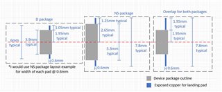
  • It looks like the SOIC (D package) is the smaller of the two packages and pitch of both packages are the same. I would probably build the footprint around the D package and just extend the landing pads to ensure the SO (NS package) can fit on top of it. 

    This is an example of what I would do to make sure both would fit. Mainly just extend the pin leg pad connections outwards. I suspect you may want to extend further than what I drew to something like 2.5mm instead of 1.95mm. 

    Remember, you will be responsible for checking the measurements and adjusting for additional overlaps. The provided looks at typical values from what I found from the datasheet. Please do your due diligence as well.

    -Bobby

  • Hi Bobby

    Thank you for reply,

    Customers are concerned that by increasing the pad size, the parts will move (shift) during mounting.

    Does this kind of phenomenon occur?

    If occur, Is there some kind of countermeasure?

    Best regards,

    Satoshi

  • Hi Satoshi,

    Customers are concerned that by increasing the pad size, the parts will move (shift) during mounting.

    Does this kind of phenomenon occur?

    I'm not that familiar with the backend manufacturing processes for boards like this. I don't know the precision of the pick and place machine, but I assume a good fabrication company would have millimeter level of precision. 

    I have a co-worker who is a bit more familiar with the PCB fabrication process. I can reassign this thread to him to see if he can comment if he thinks there could be a potential concern on this. 

    From my point of view, the electrical concern is the larger package will have some stubs which could affect the cable transmission a little.

    -Bobby

  • Hi Bobby,

    Thank you for sharing this information with your co-worker.

    Your kind support is very helpful, and I apologize for the unexpected content of the inquiry.

    I looking forward your update.

    Best regards,

    Satoshi

  • Hi Satoshi,

    During the reflow process, the surface tension of the solder will pull on the individual pins with equal tension and center the device within the overall footprint.  This assumes that there is a proper and uniform application of solder paste for each pad and some pins do not have more or less solder than other pads which would create different tension forces on the device pins which could cause the device to be pulled out of proper alignment.

    Also, as long as the device is initially "placed" in the center of the footprint, it should remain in the center of the footprint during the reflow based on the solder tension regardless of the additional pad length.  However, if the placement of the device onto the solder paste was not centered, then there is an increased risk of the device from being pulled to the stronger side.  But this is a general risk for any device on the board.

    I have seen similar dual footprint boards without any issues with a reliable board shop and good pick and place equipment that can accurately place the device in the center of the footprint and there is a uniform thickness of solder paste on each pad.  Meeting these two conditions should reduce the risk of an undesired part shift during reflow assembly.

    Regards,

    Jonathan