Part Number: DS90UB960-Q1
Hi
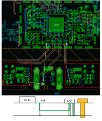
Dose ti have s-parameter requirements for fpdlink pcb or overall system? and are there some layout recommendations for fpdlink with poc section ? Because of limited pcb area,we place UB960 poc section near PCB board edge,but is it allowed for EMI and ESD performance?
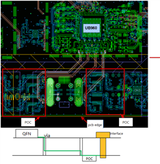
If we move 2 link poc section to TOP layer of PCB,there be more via stub ,so dose it affect the impedance performance?