This thread has been locked.

If you have a related question, please click the "Ask a related question" button in the top right corner. The newly created question will be automatically linked to this question.

DP83822I:Communication abnormality at high temperatures

Guru 19645 points
Part Number: DP83822I

If the DP83822I is used at high temperatures (over 75℃), communication errors will occur with certain ICs.

Please let me know the following four points regarding this operation.

①Would you please let me know the possible causes of the PHY internal register setting error occurring in the NG IC?

For example, is the reference voltage changing due to high temperature or some other reason?

②Are there any possible countermeasures?

③Would you please let me know if it have any concerns about communication errors other than register settings?

④If you have any other points to note when using DP83822I, please advise.

[Additional information]

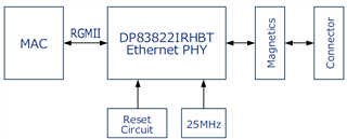
・The circuit configuration is based on the typical applications in the data sheet.

・There are differences in layout conditions between OK and NG ICs.

    - OK: VIA ×9, There is a solid pattern on the back side.

    - NG: VIA ×5, There is "not" a solid pattern on the back side.

・Even if the temperature is lowered after an abnormality occurs, the problem will not be improved.

    Restarting after lowering the temperature will return to normal.

・After normal startup, no abnormality will occur even if the temperature is raised to 75℃ or higher.

    If you restart after raising the temperature, it will fail.

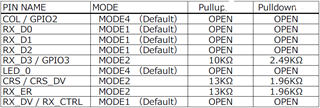
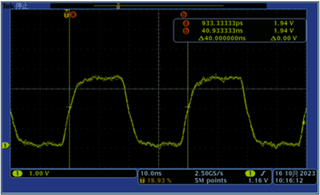
・25MHz clock is output from the [RX_D3/GPIO3] pin.

    → It is assumed that the shared pin was incorrectly set (extension register address 0x0462) during startup due to high temperature.

・There is no voltage fluctuation in BOOTSTRAP.

   ⇒We guess that the initial settings of the registers inside the PHY may be affected by something during startup at high temperatures, causing an error.

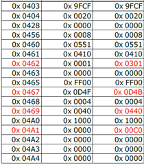
・The following is a comparison of registers for OK/NG. (Left: OK, right: NG)


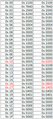
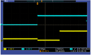
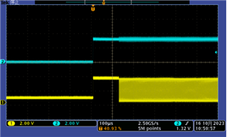
・The [RX_D3/GPIO3] waveform of OK/NG is shown below. (Left: OK and 0x0462 data is 0x0001, right: NG and 0x0642 data is 0x0301)

    *Blue: PHY reset, Yellow: RX_D3/GPIO3


→Enlargement of NG waveform (25MHz output)

Best regards,

Satoshi

  • Hi Satoshi,

    It appears off of the strapping the LED0 is being set into mode 2 which is unideal. This will cause PHY to go into test mode as noted in section 8.5 of datasheet. I would advise probing the line at powerup to understand what is happening at high temperature vs normal temperature and see if the strap is being read correctly by the PHY or if the voltage is being altered in some sort of way.

    Could you also please show the differences in the layout of the DAP, and provide schematic of PHY for quick check?

    Sincerely,

    Gerome

  • Hi Gerome

    Thank you for reply,

    In the customer's settings, LED_0 should be set to MODE4 (Default), but is it being shifted to MODE2 for some reason?

    ・BOOTSTRAP settings are as follows.

        Address: 0x0467 read bit1:0→0b11 (11=MODE4 in datasheet Table78)

    (1) Would you please let me know what does "LED_0 is MODE2" mean?

    (2) I can't find any description of "TEST MODE" in Section 8.5 Programming.

    Would you please tell me where it is written (page number)?

    About "probing the line" that you advised,

    Is it correct to understand that this is a confirmation of the BOOTSTRAP setting waveform?

    We are requesting the circuit diagram etc. from the customer, so please wait for a while.

    Is it possible to share confidential information such as circuit diagrams via email or private massage?

    Best regards,

    Satoshi

  • Hi Satoshi,

    This is an internal test mode. I cannot disclose anything more outside of this.

    Yes, this is to confirm that the bootstrap waveform is correct at this high temperature. Please send via DM.

    Sincerely,

    Gerome