


Part Number: TCA6408A-Q1
Dear TI experts,
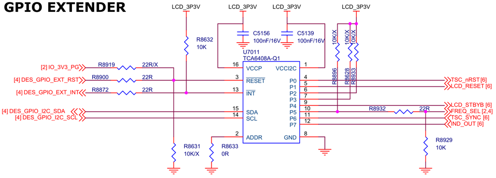
My customer made their first schematic with TCA6408A-Q1. Could you review the schematic below?
Best regards,
Chase
Part Number: TCA6408A-Q1
Dear TI experts,
My customer made their first schematic with TCA6408A-Q1. Could you review the schematic below?
Best regards,
Chase
