This thread has been locked.

If you have a related question, please click the "Ask a related question" button in the top right corner. The newly created question will be automatically linked to this question.

DP83825EVM: near-end loopback fails

Part Number: DP83825EVM
Other Parts Discussed in Thread: USB-2-MDIO

I am trying to use a pair of DP83825EVM boards to add two 10baseT interfaces to an FPGA evaluation board.  I have added zero-ohm resistors in the pads connecting RMII to J9 and connected J9 to suitable FPGA board ports, with the FPGA programmed as a rudimentary MAC.  I have added a zero-ohm resistor at R46, removed R41, and wired a 50MHz clock from the FPGA board to J14 via twisted pair with 100-ohm impedance.  I have removed R53 and R54 and wired FPGA IO to J10 to support register read/write from the FPGA.  I have added a 2.49K pullup to CLKOUT to assign the RXDV pin function. I have added a zero-ohm resistor at R45 to set slave mode.


For initial testing I have provided a 10Mbps packet generator at the RMII RX port and am running near-end loopback testing. For this I have written the following registers:

Register 0x0000: 0x0100

Register 0x0017: 0x0081

Register 0x0016: 0x0001, 0x0002, 0x0004 for the various near-end loopback functions.


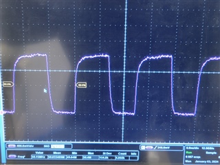
Applying test packets to the RMII RX port, I see RMII TX signals returned as follows:

0x0001: signal

0x0002: no signal

0x0004: no signal

 So I am evidently losing loopback at the PCS output and onward. What might I be doing wrong?

  • Hello Diversified Design,

    Thank you for provided your register configuration and explaining your test set up. Please help me understand a few more things about your set up.

    Could you provide a block diagram of your set up and show where you're connecting the packet generator and which 825EVM is being configured into loopback?

    I also want to confirm that the RX lines are OUTPUTS from the PHY.

    Regards,

    Alvaro

  • Here's a block diagram for the connections to, and modifications of, the DP83825EVM board.  (Yes, I noticed the RX/TX typo after sending.)

    I hope you can expand this clip sufficiently to read it.

  • I see you can just click on the clip to expand it.  Excellent.

  • Hello,

    Thank you for your response. Please note the US offices are closed for Thanksgiving Holiday and will look to reopen next week.

    Sincerely,

    Gerome

  • It's been a week since Thanksgiving, haven't heard back; hoping for some help on this urgent matter.

  • I have started a separate effort to uncover the problem; both efforts are now running in parallel.  Ultimately I need to get two DP83825EVM boards working with my FPGA evaluation board (as shown in block diagram above) but I also bought a new DP83825EVM to try factory-fresh, no modifications.  I see that the DP83825EVM has three resistors (R9, 10, 17) which should provide a default line-loopback function.  I tried connecting the new DP83825EVM  to a Win11 computer configured for a fixed IPV4 address and running Wireshark.  The PHYs connected, and Wireshark saw the usual startup messages from the computer's assigned IP address.  But Wireshark did not show these messages bouncing back from the DP83825EVM .  Should this have worked?

  • Continuing with this new unmodified DP83825EVM and using USB-2-MDIO for register R/W and running Wireshark on a connected computer, I wrote 0x0700 to register 0x0016 in an attempt to turn on continuous PRBS packets, which I hoped to see in Wireshark.  This control register write does illuminate the activity LED on the connected computer, and writing 0x0000 to 0x0016 extinguishes the activity LED.  But Wireshark sees nothing. Shouldn't I see the PRBS packets?

  • Hi Diversified Design,

    Apologies for the wait, I was out of office from Nov 23-29, but I am back now. Thank you for providing the block diagram, as it 

    Before diving into details I want to confirm the connection between the FPGA and the 825EVM, how are they being connected? 

    Regards,

    Alvaro

  • Hi Alvaro -

    Referring to the block diagram: I stuffed resistors R12, 14, 16, 11, 13, 15 and used a ribbon cable from J9 to the FPGA evaluation board.  I also removed resistors R10, 9, 17 to eliminate the factory-installed loopback.

    -DD

  • Hi DD,

    Thank you for clarifying. Are you able to probe these signals on both ends, to confirm the waveforms are being sent cleanly(TXD0/RXD0)? 

    Regards,

    Alvaro

  • Yes, they look good.  So does the 50MHz clock.  But if you don't see anything else wrong with this setup - eg. the strapping, the register setup, or the expectations - you could skip ahead to the later experiments I've outlined which don't use any external signals at all, or any rework of the board.  Maybe something there could shed some light.

  • Hi Diversified Design,

    I want to clarify a few things. With regards to enabling loopback modes, when you're writing Reg 0x16, are you writing 0x1, 0x2, & 0x4 all back to back? This would change the type of loopback each time. Please note that setting Reg 0x16 = 0x0004 enabled Digital Loopback, which is only supported in 100Base-TX, not in 10Base-Te. 

    Register 0x0000: 0x0100

    Register 0x0017: 0x0081

    Register 0x0016: 0x0001, 0x0002, 0x0004 for the various near-end loopback functions.

    On the unmodified board, you tried to enable packet Generation, but I believe your register writes were incorrect. Bits 13:12 In Register 0x16 need to be enabled to start packet generation. Try writing Reg 0x16 = 1102. It is unclear in the data sheet but I believe Bits 10:9 are status bits, meaning they can only be read, not written. Another thing that is unclear, is that for Packet generation to work, a loopback needs to be enabled. In the register write I suggested, 0x1102, I selected PCS loopback.

    Continuing with this new unmodified DP83825EVM and using USB-2-MDIO for register R/W and running Wireshark on a connected computer, I wrote 0x0700 to register 0x0016 in an attempt to turn on continuous PRBS packets

    Please let me know if this helps.

    Regards,

    Alvaro

  • Thanks, Alvaro -

    I hope to get a chance to try some of your ideas this afternoon.  In answer to your question about loopback, the various register 16 writes were done one at a time, with results checked each time.  Interesting that 0004 is only defined for 100M; I had evidently misread this.  But what about 0002? Should it have worked?

    Also, could you give the "line loop back" experiment some thought?  I'm referring to the experiment where I leave R9, 10, 17 in place and expect to see loopback on the line side from my computer through the PHY and back to the computer.  Should this work?  (No board mods, no register writes, letting it auto-negotiate.)

  • Hi Diversified Design,

    MAC <-> PHY <-> PC

    After re-reading the datasheet, I can see how this is not immediately clear. PCS, Digital, and Analog loopbacks affect the MII side of communication. So the data path would be MAC -> PHY -> MAC.

    In your experiment, you want PC -> PHY -> PC, correct? If so, then external/reverse loopback is the one to use.

    Regards,

    Alvaro

  • Hi Alvaro - 

    Thanks for your help.

    I think I have created some confusion by presenting three different test cases all at once. 

    In the first case, I am working with a modified evaluation board (mods described and diagrammed) and testing near-end loopback functions of the PHY by driving 10Mbps signal into TX RMII and looking for signal at RX RMII.  I get signal with Reg16 = 0001, but not with Reg16 = 0002 or 0004.  I understand that 0004 is only defined for 100M, so would not expect return signal there.  But what about for Reg16 = 0002?  Shouldn't that work?  If 0001 works and 0002 does not, what could be wrong? Could the PCS stage be fining some fault with my RMII signal that the MII stage would not be sensitive to?

    In the second case, I am working with a factory-fresh evaluation board and trying to use the external loopback function that I believe is created by R9, R10, R17 external to the PHY on the evaluation board. In this case I am using only default register settings.  I am connecting the line side of the evaluation board to a PC with Wireshark running, and watching what happens when I connect the Ethernet from PC to evaluation board. When the Ethernet connection links, I see a series of PC-generated messages on Wireshark, which is the usual case whenever the PC connects to anything else.  But due to the loopback function set up by these three resistors on the evaluation board, I would expect to also see these same Ethernet messages echoed back to the PC.  I do not.  Do you think I should?

    In the third case, I am again working with a factory-fresh evaluation board.  Again the evaluation board is connected to a PC.  But in this case I write 7000 to register 16 to turn on PRBS packet generation. (I see I had a typo in my description which incorrectly specified writing 0700.)  I've also tried writing 3000 to register 16 (which is bits 12, 13 only).  In each case, I see the Activity LED on the PC Ethernet port light, so I know some kind of traffic is getting generated by the PHY. But I would expect to see PRBS packets showing up on Wireshark, and I do not.  Do you think I should?

    I recognize that these last two cases could be interpreted as questions about Wireshark and not about DP83825EVM.  If this is outside your expertise, I apologize. I'm using Wireshark to keep the setup as simple and general as possible by avoiding any custom software. Do you have any alternate suggestions for monitoring operation?

    -DD

  • Hi DD,

    Thank you for clarifying.

    Case 1:

    I'm not sure if PCS Output (0x2) has an issue or not with 10 Mbps, but doesn't PCS input validate the signal you were trying to test?

    Case 2:

    Could you try this test again, PC (Wireshark) -> PHY, where Wireshark is generating and sending packets, except this time we configure the PHY into reverse loopback (Reg 0x16 = 0110). This would loop back the packets internally within the PHY, instead of sending them through the MAC pins where R9, R10, and R17 are connected.

    I tried this in lab with a packet generator and it worked, I enabled 10 Mbps by de-advertising 100M modes (Reg 0x4 = 0061)

    This didn't work when data was sent through R9, R10, and R17.

    Case 3:

    The PRBS Generator on the PHY makes random data and not packets, there is a difference and this may be why Wireshark isn't seeing anything.

    Regards,

    Alvaro

  • Thanks, Alvaro -

    Your answer to case 3 is instructive: I had the incorrect impression that the PRBS generator would encapsulate PRBS as payload within ethernet packets.  I now know this is not the case. 

    Regarding case 1, I'm using these simple tests in part to verify my own RMII packet generator, since it too is unproven. I took the failure for my packets to loop back from PCS as a possible indication that my packet generator was improperly designed. Do you have lab capability to try the PCS loopback at 10Mbps with a known-good packet generator so we can see if the loopback failure is caused by a fault in my packet generator or just an undocumented feature of the PHY at 10Mbps?

    As for case 2, that's an interesting idea. I'll give it a shot.

    -DD

  • Hi DD,

    Please let me know how the Case 2 experiment goes. I can try Case 1 on Monday and will get back to you.

    Regards,

    Alvaro

  • HI Alvaro -

    I have tried your Case 2 experiment.  Again I used the PC connection messages as the packet source because I can't seem to figure out how to use Wireshark as a packet generator.  (Can you tell me?). The PC generates a wide range of packet types upon making connection.  With Reg16=0110, Wireshark captures at least twice as many messages as with Reg16-0000. Interestingly I do seem to find some packet types repeated with just the "resistor loopback" (Reg16=0000). So I guess the PHY is looping back at 10Mbps with both reverse loopback methods; just more packet types are seen by Wireshark one way than the other.  Obviously there's a lot going on here that I don't understand, likely largely involving the inner workings of the PC's TCP/IP stack.  Let's call this a "pass" for the PHY in both reverse loopback modes, both restricted to 10Mbps and with auto-negotiation.  I just don't have a well-enough controlled test setup to make what's going on obvious.

    I'm still very much interested to see what you get with a known-good packet generator in Case 1. 

    -DD

  • Hi DD,

    The boards I have at the moment need some rework before I can attempt this experiment. Please allow me to the end of the week to make the board changes and run the experiment. 

    Thank you for your patience,

    Alvaro

  • Hi DD,

    I managed to get my set up working and tested various loopbacks. I didn't have a board with an SoC and DP83825 to recreate your setup exactly, instead I used two DP83825EVMs and configured them into RMII repeater mode. I used a packet generator to send packets, and set the final board into a loopback mode to see if the packets made it back. More details on the modifications made to each board is provided below.

    Packet Generator <--- Ethernet Cable ---> DP83825EVM <---RMII Repeater---> DP83825EVM (enable loopbacks here)

    Both boards were set to 10 MBPS by de-advertising 100 MBPS modes and keeping auto-negotiation enabled; i.e. setting Register 0x4 = 0061 (default was 0x01E1).

    For the purpose of validating the MAC connection, Reg 0x16 = 0101 (PCS Input Loopback) would consistently work, but PCS Output loopback didn't.

    Even better, I found that Reg 0x0000[14] (MII Loopback enable) worked the most consistently. The register description advises an additional write to Reg 0x16 if using MII loopback.

    Please note that I will be on Holiday vacation starting next week, Dec 18th-27th. I hope this clears up any issues and helps you validate your design.

    Happy Holidays!

    Setup:

    2x DP83825EVM

    EVM Board #1

    • Add 0Ω to
      • R11-R16
      • R45-R46
    • Install SMA CLK_IN Connector
    • Remove
      • R9, R10, R17
      • R36, R41

    EVM Board #2

    • Add 0Ω to
      • R11-16
    • Install SMA Connector to CLK_OUT
    • Remove
      • R9, R10, R17

    Regards,

    Alvaro

  • Hi Alvaro -

    I hadn't mentioned it before, because I was trying to keep things simple - but the end use of my design is to connect two Ethernet ports through a proprietary link that will be implemented by two FPGAs, one on the RMII side of each PHY.  You have now built a test setup very similar to this.  And from the standpoint of loopback testing, you have replicated my results - including the loopback tests that have worked and those that have not.  There are only two steps left to prove - or not - that this link can work:

    1. The first step is just a quick test with what you already have set up: A colleague has been doing some testing on this same evaluation board model as well, and has found that sometimes he will set up registers for 10Mb, and the link will start and run briefly at 10Mb and then switch to 100Mb!  Could you please so a couple of quick oscilloscope tests and verify that your RMII is in fact switching at 5Mbps and that the clock between boards is really 50MHz?

    2. The second step is more of a pain, but you've already done most of the work: In my application, since the two FPGAs and PHYs will be at opposite ends of an analog link that can't support a clock, it is necessary that BOTH PHYs run in slave mode. Would it be feasible for you to convert the second PHY to slave mode and drive both PHYs from a common 50MHz clock source?  It's a small detail, but this would make your test circuit fully compatible with my requirements and prove that it can be done. 

    Thanks

    DD

  • Hi DD,

    I'm glad my set up has been a helpful validation result for you. Like you said, I believe I can get the results for 1.  soon, but I am skeptical about the setup for 2. The setup I have with 2 EVMs connected with jumper wires is already far from ideal. I'll try splitting a clock signal from a waveform generator using a bnc-t, then using an BNC to SMA convertor so that I can connect it to the boards. 

    Please allow me till the end of this week to modify the board and debug the setup, I suspect I will encounter many problems along the way.

    Regards,

    Alvaro

  • Hi Alvaro -

    I hear you regarding the physical difficulty of making these modifications; been there!  I am grateful you're soldiering on.

    -DD

  • Hi DD,

    I did your 1. test can confirmed the shared clock coming from the RMII_Master board is indeed 50 MHz. Please see the pictures below. However I'm not sure what you mean by the PHY switches to 100 Mb. How do you know that this is happening?

     50 MHz CLKOUT signal from RMII Master

    Figure 1 CLKOUT Signal from RMII_Master

    Figure 2 - Picture of setup: SMA CLKOUT cable directly going to Channel 3 of Oscilloscope

    Regards,

    Alvaro

  • Hi Alvaro -

    Thanks for this check; it's certainly encouraging.  While you've got the scope out, could you please humor me and also take a peek at one of the RMII lines while the system is operating and double check the expected data rate for 10Mbps (5Mps per line)?  I did not witness this personally, but have a colleague working at another facility who said he thought he had this running correctly (evidence being proper register setup and good data transfer) only to find later that the PHYs did not stay at 10Mbps but in fact moved to 100Mbps within seconds after starting up at 10Mbps.  He found this by directly monitoring the RMII signals. That's the only information I have.  But if it's only a matter of taking a quick peek at the RMII at J9 during operation, I'd like to be able to check that concern off the list.

  • Hi DD,

    I checked the RX_Data lines but there isn't really a way to tell how fast the data rate is just from this waveform. The 50 MHz ref_clk is used for both 100M & 10M, and for 10M it is 10 times faster than the data-rate. So to account for this, data on the RX lines are sampled at every 10th cycle. Please note that I have not begun the rework necessary to begin experiment 2. , since I will have to convert the RMII_Master board into a RMII_Slave.

    Regards,

    Alvaro

  • Hi Alvaro -

    Thanks for noting that the 50MHz clock will not expose the data rate.  That makes the MII observation more important.  I've found if I just look at one of the MII data lines for a while during packet transfer I can see what the minimum time between transitions is.  This will be the data period and should of course be 20ns for 100baseT and 200ns for 10baseT on RMII. Might be useful to use infinite persistence on the scope. 

    -Ken

  • Hi Ken,

    You're right. It was 20 ns at 100Base-T and 200 ns at 10BaseT. However I didn't encounter a switching between the speeds. 

    I used Register 0x10[1] as a sanity check for Speed, and it matched what I was reading at the oscilloscope. The speed was set by the Data Generator, but if you wanted to disable 100Base-T you could de-advertise it by writing Reg 0x4 = 0x61. 

    Regards,

    Alvaro

  • Thanks for that check, Alvaro. Looks like you've definitely got #1 going at 10Mbps.

    Have you given up on #2?

    -DD

  • Hi DD,

    Was waiting for confirm the 10/100 switching issue first. There's no reason that the DP83825 shouldn't be able to work in a RMII Slave repeater application. My skepticism comes from getting it to work on the EVM boards with the jumper wire connections and split clock source. Nonetheless I can begin making the board changes and try this out. Can have results ready before the end of this week.

    Regards,

    Alvaro 

  • Hi DD,

    Just wanted to give an update, board modifications have been made, will go into lab and bring them up today. The goal is to have a more detailed response by end of week.

    Regards,

    Alvaro

  • Hi DD,

    I regret to inform that the setup with the 2 EVMs did not work. Register access was not cooperating, nor was sustaining link. Again, I want to reiterate that the DP83825EVM is not suitable for a RMII Slave to RMII Slave application. 

    Aside from this setup is there anything else I can help you with?

    Regards,

    Alvaro

  • Hi Alvaro -

    This is disappointing, but I thank your for soldiering on as long as you did; I know this went far afield of what you'd normally expect to encounter. 

    -DD