This thread has been locked.

If you have a related question, please click the "Ask a related question" button in the top right corner. The newly created question will be automatically linked to this question.

SN65DSI86: How To Enter PHY_TEST_PATTERN

Part Number: SN65DSI86
Other Parts Discussed in Thread: TEST2

Dear TI,

I did the following after TEST2 was pulled up.

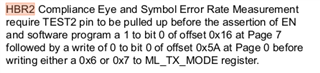
chose operation:
[0]: HBR2 Compliance Eye Pattern
[1]: Symbol Error Rate Measurement Pattern
[2]: 80-bit Custom Pattern
[3]: Other: Setting Reg
[4]: Other: Read DPCD
: 0
set reg: [0A] = 00000010
now reg: [0A] = 00000010
we will use refclk 1
set reg: [94] = 10000000
now reg: [94] = 10000000
set reg: [93] = 00110100
now reg: [93] = 00110100
set reg: [FF] = 00000111
now reg: [FF] = 00000111
set reg: [16] = 00000001
now reg: [16] = 00000001
set reg: [FF] = 00000000
now reg: [FF] = 00000000
set reg: [5A] = 00000100
now reg: [5A] = 00000101
set reg: [0D] = 00000001
now reg: [0D] = 00000001
set HBR2_COMPEYEPAT_LENGTH reg (260): 260
set reg: [98] = 00000001
now reg: [98] = 00000001
set reg: [97] = 00000100
now reg: [97] = 00000100
now ENCH_FRAME_PATT = SR BF BF SR or BS BF BF BS
[0]: SR BF BF SR or BS BF BF BS
[1]: SR CP CP SR or BS CP CP BS
choose ENCH_FRAME_PATT (0): 0
set reg: [5B] = 00000000
now reg: [5B] = 00000000

[0] = Pre-emphasis level 0.
[1] = Pre-emphasis level 1.
[2] = Pre-emphasis level 2.
[3] = Pre-emphasis level 3.

set Pre-Emphasis Level (recommend 1): 0
set reg: [93] = 00110100
now reg: [93] = 00110100

[0] = Voltage swing level 0.
[1] = Voltage swing level 1.
[2] = Voltage swing level 2.
[3] = Voltage swing level 3.

set VOD level (recommend 1): 0
set reg: [94] = 10000000
now reg: [94] = 10000000

[0] = Post-Cursor2 Level 0 (0 dB) (Default)
[2] = Post-Cursor2 Level 1 (0.92 dB)
[4] = Post-Cursor2 Level 2 (1.94 dB)
[6] = Post-Cursor2 Level 3 (3.10 dB).

set post cursor2 (recommend 0): 0
set reg: [95] = 00000000
now reg: [95] = 00000000
set reg: [96] = 00000110
now reg: [96] = 00000110

now bridge reg is

00000000: 3638 4953 4420 2020 0200 8200 0001 0000 68ISD ........
00000010: 3e00 6500 0000 0000 0000 0000 0000 0000 >.e.............
00000020: 0000 0000 0000 0000 0000 0000 0000 0000 ................
00000030: 0000 0000 0000 0000 0000 0000 0000 0000 ................
00000040: 0100 0000 8000 0000 0000 0000 0000 0000 ................
00000050: 0000 0000 0000 2000 40e4 0500 1000 9000 ...... .@.......
00000060: a060 a400 0000 0000 0000 0000 0000 0000 .`..............
00000070: 0000 0000 0001 0301 9009 0000 0000 0000 ................
00000080: 0000 0000 0000 0000 001f 7cf0 c107 1f7c ..........|....|
00000090: f0c1 0734 8000 0604 0100 0000 0000 0000 ...4............
000000a0: 01ff ff00 0000 0000 0000 0000 0000 0000 ................
000000b0: 0478 acac 086c 9c9c 0c5c 5c5c 0c0c 0c0c .x...l...\\\....
000000c0: 3f3f 0f00 0000 0000 0000 0000 0000 0000 ??..............
000000d0: 0000 0000 0000 0000 0000 0000 0000 0000 ................
000000e0: 0000 0000 0000 0000 0000 0000 0000 0000 ................
000000f0: 0002 0000 0102 0000 0000 0000 0000 0000 ................

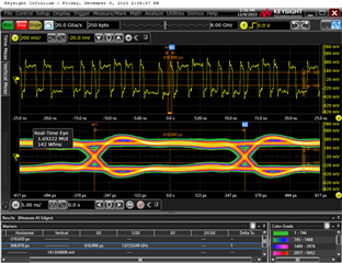
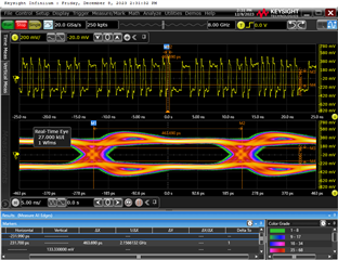
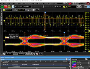
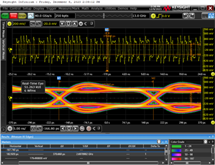
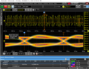
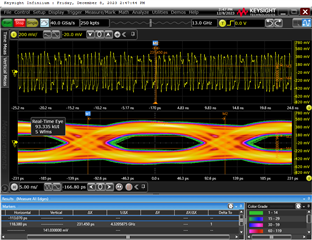
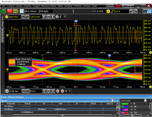
I set data rate hbr, but waveform is hbr2(5.4Gbps)

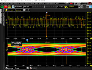
if i set data rate is 1.62Gbps, the waveform will be 4.32Gbps

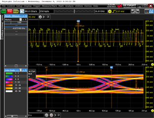
I found that the waveform appeared when I was doing DP LOCK(0x0D), and I wasn't even sure if mode set to HBR2(0x96) worked because I didn't see a significant change。

I read the spec carefully and I couldn't find anything wrong with it

  • Have you tried any other setting in the 0x94 register? It seems that frequencies are not lining up correct?

    try running this script for the HBR2 pattern and changing the 0x94 register after confirming that the pattern displayed is an HBR2 pattern. 

    This is an aardvark script, but you can also read the registers set in this an translate to your I2C controller

    <aardvark>
        <configure i2c="1" spi="1" gpio="0" tpower="1" pullups="0"/>
        <i2c_bitrate khz="100"/>
    
    ======DISABLE HPD======
       <i2c_write addr="0x2D" count="1" radix="16">5C 01</i2c_write> <sleep ms="10"/>
    
    ======Clear Status CSR======
    <i2c_write addr="0x2D" count="10" radix="16">F0 FF FF FF FF FF FF FF FF FF FF</i2c_write> <sleep ms="10"/>
    
    ======Configure DP LUT======
    <i2c_write addr="0x2D" count="1" radix="16">	B0	04	</i2c_write> <sleep ms="10"/>
    <i2c_write addr="0x2D" count="1" radix="16">	B1	78	</i2c_write> <sleep ms="10"/>
    <i2c_write addr="0x2D" count="1" radix="16">	B2	AC	</i2c_write> <sleep ms="10"/>
    <i2c_write addr="0x2D" count="1" radix="16">	B3	AC	</i2c_write> <sleep ms="10"/>
    <i2c_write addr="0x2D" count="1" radix="16">	B4	08	</i2c_write> <sleep ms="10"/>
    <i2c_write addr="0x2D" count="1" radix="16">	B5	6C	</i2c_write> <sleep ms="10"/>
    <i2c_write addr="0x2D" count="1" radix="16">	B6	9C	</i2c_write> <sleep ms="10"/>
    <i2c_write addr="0x2D" count="1" radix="16">	B7	9C	</i2c_write> <sleep ms="10"/>
    <i2c_write addr="0x2D" count="1" radix="16">	B8	0C	</i2c_write> <sleep ms="10"/>
    <i2c_write addr="0x2D" count="1" radix="16">	B9	5C	</i2c_write> <sleep ms="10"/>
    <i2c_write addr="0x2D" count="1" radix="16">	BA	5C	</i2c_write> <sleep ms="10"/>
    <i2c_write addr="0x2D" count="1" radix="16">	BB	5C	</i2c_write> <sleep ms="10"/>
    <i2c_write addr="0x2D" count="1" radix="16">	BC	0C	</i2c_write> <sleep ms="10"/>
    <i2c_write addr="0x2D" count="1" radix="16">	BD	0C	</i2c_write> <sleep ms="10"/>
    <i2c_write addr="0x2D" count="1" radix="16">	BE	0C	</i2c_write> <sleep ms="10"/>
    <i2c_write addr="0x2D" count="1" radix="16">	BF	0C	</i2c_write> <sleep ms="10"/>
    <i2c_write addr="0x2D" count="1" radix="16">	C0	3F	</i2c_write> <sleep ms="10"/>
    <i2c_write addr="0x2D" count="1" radix="16">	C1	3F	</i2c_write> <sleep ms="10"/>
    <i2c_write addr="0x2D" count="1" radix="16">	C2	F	</i2c_write> <sleep ms="10"/>
    <i2c_write addr="0x2D" count="1" radix="16">	C3	0	</i2c_write> <sleep ms="10"/>
    
    ======Pre0dB 4 lanes no SSC======
       <i2c_write addr="0x2D" count="1" radix="16">93 30</i2c_write> <sleep ms="10"/>
    
    ======L0mV HBR2======
       <i2c_write addr="0x2D" count="1" radix="16">94 E0</i2c_write> <sleep ms="10"/>
    
    ======PLL ENABLE======
       <i2c_write addr="0x2D" count="1" radix="16">0D 01</i2c_write> <sleep ms="10"/>
    
      <i2c_write addr="0x2D" count="0" radix="16">0A</i2c_write> <sleep ms="10"/>
    
       <i2c_read addr="0x2D" count="2" radix="16">00</i2c_read> <sleep ms="10"/>
    
    ======POST2 0dB ======
       <i2c_write addr="0x2D" count="1" radix="16">95 00</i2c_write> <sleep ms="10"/>
    
    ======HBR2COMPEYE PATT ======
       <i2c_write addr="0x2D" count="2" radix="16">97 04 01</i2c_write> <sleep ms="10"/>
       <i2c_write addr="0x2D" count="1" radix="16">96 06</i2c_write> <sleep ms="10"/>


    </aardvark>
    

  • After the above register Settings, I set 0x94 from 0 to HBR2, and the value 0 has the same effect as 1.

    0_1G62bps

    2_2G16bps

    3_2G42bps

    4_2G7bps

    5_3G24bps

    6_4G32bps

    7_5G4bps

  • Is this a pattern for HBR2 in these figures? How to confirm that this is the pattern of HBR2.

    Why is the waveform emitted after setting 0x0D (PLL EN) and not after setting 0x94?
    Can you provide an example diagram of the HBR2 TEST waveform?

  • Hey Li,

    I cannot confirm the test pattern by looking at the data on a scope.

    There are two ways to verify the test pattern in correct:

         1) use a protocol analyzer

         2) Use compliance software

    The PLL EN is the enable for the output (DP) clock. This device will not output anything until PLL_EN is set as the clock is a prerequisite to output data. Changing the frequency will change the internal clock multipliers/ dividers for the TX side (PLL_EN side as well). 

  • The HBR2 test patterns you have shown are over equalized resulting in the bump for the eye. Lower the equalization settings to improve the Eye diagram. 

  • Hey,

    Don't we have to set this up according to the documentation? Are there any other register Settings for HBR2 TEST?

    Thanks.

  • Dear Ti,

    The Settings you gave me earlier will cause an oscilloscope EDP automatic test error.

    Does the manually set TX swing code and post1 pre-emphasis need to be aligned with the actual edp panel training parameters?

    Thanks.

  • To confirm the test pattern is correct please very using the method mentioned above. Make sure the data rate, pre-emphasis and swing are all aligned with the test you are taking. you can manually change these parameters in the script