A related question is a question created from another question. When the related question is created, it will be automatically linked to the original question.
If you have a related question, please click the "Ask a related question" button in the top right corner. The newly created question will be automatically linked to this question.
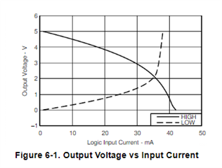
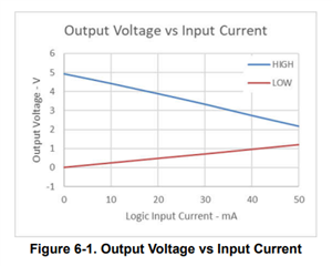
The move to 300 mm wafers involved a redesign of the die (PCN# 20230814006.1). Apparently, the new design has a higher drive strength. (The voltages are still inside the limits guaranteed by the datasheet, and the differences are noticeable only when you exceed the absolute maximum rating of 20 mA.)
Yes - the redesigned version of this part does have a slightly higher drive strength - it is still bound by the same datasheet conditions that the legacy device is, but under typical operating conditions you may see a slight increase in drive strength. We have noticed that the 300mm wafer updates do have some minor improvements - because our new process is better
I will note though that we still have a mix of older and newer material in circulation so customer may get older material still so any design should still be okay w.r.t. to max/min conditions listed in datasheet to ensure compatibility.
There shouldn't be any issues using newer material in systems designed with the older material - but there may be some marginal improvements at a part level - but it probably won't be very noticeable at a system level.
Please let me know if you have any other questions!