This thread has been locked.

If you have a related question, please click the "Ask a related question" button in the top right corner. The newly created question will be automatically linked to this question.

SN65DPHY440SS:Lane 1 MIPI communication error

Part Number: SN65DPHY440SS
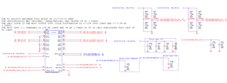
I am using a 1 lane dsi application.
There were no problems with MIPI communication.
However, sometimes the display panel does not turn on.

-
It is being output through DB0P.
-
I checked that VCC is 1.8V.
-
When normal, check the eye diagram and keep your eyes wide open.
- It is a structure that cannot take the waveform in a situation where it is not turned on.
Can you tell me what to check?


  • Hello, Kim,

    Can you send me your schematic so I can take a look at that first?

    Also, do you have a scope that you can show me the clock and data signals into and out of the retimer?

    Thanks,

    Zach

  • Heello, Zach

    The schematic is as follows:

    I2C is not used, and the settings are as follows.

    You can check the signal input and output of the retimer through the scope.

    There were no problems with the LP and HS sections.

    It is not possible to check with Scope in the environment where the problem occurs.

    When the problem occurred, modifying the clock phase did not solve the problem.

    In this case, the only way to fix the problem is to turn the retimer off and then back on.

    If you know of a way to check further, please advise.

    Thank you.

    Have a good day

  • Hello,

    What is the data rate are you running? Is this a CSI or DSI application? What is the length of the output trace?

    Can you provide the insertion loss from the CPU to the input of the device? 

    The configuration pin settings are all set to VIL. How was this decided? 

    Thanks,

    Zach

  • HI Zach

    Data rates are less than 1 Gbps.

    The application is DSI.

    All configuration pin settings are LOW.

    We use multiple channels. Use multiple retimers.
    So the length of each channel is different.
    The short channel is 24mm and the long channel is 89mm.
  • Kim,

    Please try reconfiguring the configuration pins to see if this fixes the problem. You might try leaving each configuration pin floating and pulling ERC high.

    Also, could you take screenshots of the oscope of the input channel and the output channel of lane 0?

    Could you try using DA1P and DA1N pins instead of the lane 0 pins? If you want to continue using lane 0, then you need to make sure that you have a LP RX on the output of the DB0P and DB0N and a LP TX on the input of the DA0P/N pins.

    Thanks,

    Zach

  • Hi, Zach
    There is no DISPLAY PANNEL at the RETIMER output terminal.
    At this time, the problem occurs intermittently, and the cause of this problem is believed to be LANE0 LP TX not shutting down as mentioned in the forum.
    When reproduced in a similar form, it was confirmed that 260mV LEVEL was maintained in DBPP/N, and normal operation was observed in RSTN LOW/HIGH.
    So we want to reproduce this method to see if it is correct. I would like to inquire if there is a way to create a situation where LP TX does not terminate or RETIMER behaves abnormally.

  • Hi, Kim,

    If there is no LP RX at the output then you will see the retimer behaving abnormally. Since you will not be able to exit LP state and enter the HS state.

    Thanks,

    Zach

  • Hello.

    What is an unusual situation?
    Can I check the waveform or level of Lane0?
    In most cases, it is OK to not have an LP RX on the output and then connect the LP RX back to the output.
    This time, we want to create an abnormal state through RSTN control and check whether the current problem has been improved.

  • Hi, Kim,

    The lane 0 is special as stated above. You should use lane 1 if you are not connected to an LP RX.

    Thanks,

    Zach

  • Hi, Zach

    Use only LANE0.
    Use by connecting the DISPLAY PANNEL connected to LANE0.
    However, we confirmed that RETIMER operates abnormally when the DISPLAY PANNEL is not connected, and we considered controlling RSTN to improve this. I want to make sure this is the right path.
    So I'm wondering how to force RETIMER into an abnormal state.

  • Hello, Kim,

    Why do you want to force the retimer into an abnormal state? 

    To prevent an abnormal state, you will need to make sure that the Display panel you connect at the output of LANE0 has an LP RX.

    Thanks,

    Zach

  • Hello, Zach

    The reason for forcing the retimer into an abnormal state is to create a problem state and then check whether the problem has been resolved through RSTN control.

    I came up with this method because it is not common for the retimer to become abnormal.

    The symptom has been reproduced and resolved, so there is no need to check further.

    As you advised, this occurred because the Display Panel was not connected to Lane 0.

    Can RSTN be controlled using the push-pull method?

    Control was successful with the open drain method, but the push pull method was not successful.

    I would like to inquire about the current push-pull method because it is easy to apply.

  • Hello,

    Because of the holidays, TI E2E design support forum responses may be delayed from Dec. 25 through Jan. 2. Thank you for your patience.

    I am looking at this now and will get back with you shortly.

    Thanks,

    Zach

  • Hello,

     The two ways of implementing the reset to this device are shown in the 8.2.2.1 Reset Implementation section of the datasheet.

    There is the External Capacitor Controlled RSTN or the RSTN Input from Active Controller using an open drain driver.

    Thanks,

    Zach