Part Number: TUSB4041I
Hi
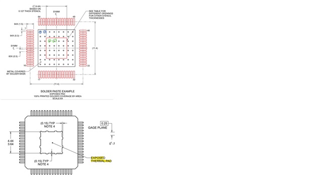
Confirm the following questions: as shown below
1. The red part should be the bare copper area
2. The blue and green circles should indicate Gnd Via
3. Is the via in the blue circle necessary? What is its function? I think it is not in the IC EXPOSED THERMAL PAD area