This thread has been locked.

If you have a related question, please click the "Ask a related question" button in the top right corner. The newly created question will be automatically linked to this question.

TLK10081: 8 GBps Ethernet over fiber bridge

Part Number: TLK10081
Other Parts Discussed in Thread: DP83869HM, DP83869

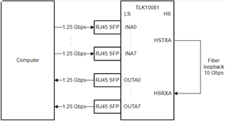
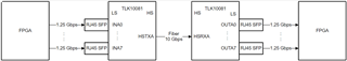
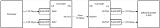
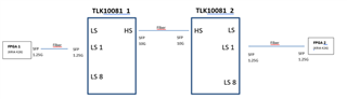
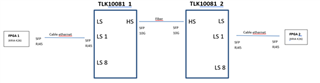
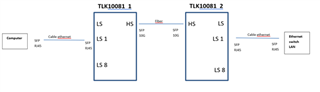
We need to connect 8 lines 1Gbps ETHERNET (SFP)  through a 10 Gbps Fiber link.

We have choosen TLK10081 for this.

Is it posssible to get a full configuration for this. We have tested many configuration of HS/LS, PLL/VCO ...

CLK_0 and CLK_1 are 10ppm TCXO (both side). CLK_0 is 125 MHZ, CLK_1 is 156.20 MHz.

It works with loopback (with fiber), but 8B/10B errors appear with fiber link (2 boards).

Best regards.

  • Hi,

    Can you clarify the data rates you are using? Typically 1G ethernet has a line rate of 1.25 Gbps with 8b/10b encoded data. Typically 10G ethernet has a line rate of 10.3125 Gbps with 64b/66b encoded data. Are these the line rates you are using? Or is it truly 1 Gbps and 10 Gbps?

    It's difficult for me to provide 1 full configuration as there are many factors that will influence how the registers should be configured. Can you share a full register dump? I can review your settings and provide recommendations.

    Can you additionally provide a system block diagram for better clarification on your setup?

    Best,

    Lucas

  • HI Lucas,

    First I wish you an happy new year.

    On Low Speed side, we have 8 sfp/RJ45 devices (framing 1000BaseT), and on HS side (Chan A) we have an 2.5 Gbps SFP+ fiber optic (1310nm/1270nm).

    On LS Side, we are using only 7 GBe channels (8th is for debug). We doesn't want any specific protocol on HS side. We just want to send data over 1 fiber.

    Best regards.

  • Oups on HS side is using a 12.5 Gbps SFP+

  • Hi Gilles,

    TLK10081 supports up to 10Gbps on the HS side. Do you mean that your SFP+ module supports up to 12.5Gbps, but is operating at 10Gbps for this application? Based on your description, I believe you have 8 SFP modules operating at 1.25Gbps (8b/10b encoded 1GbE) which are being aggregated into an SFP+ module operating at 10Gbps (8b/10b encoded). I believe these rates work out mathematically (8 * 1.25Gbps = 10Gbps). Can you confirm if this is correct?

    You mentioned you got the TLK10081 working with fiber loopback. Does this mean you don't see errors when transmitting data to the LS inputs, looping HSTX to HSRX, and checking errors on the LS outputs?

    Can you share a full register dump for me to review which settings you are using and if there are any configuration mistakes?

    Best,

    Lucas

  • Hi Lucas,

    When loopback HS side, no error is detected and both Rx and TX are synchronized.

    Best regards.

    PS: Please find a dump of registers for both side (phys_address 0X1 and 0x2

    ==================================================== 0x00
    read mdio phy_address 0x1 reg_address 0x0 : 0x610
    read mdio phy_address 0x2 reg_address 0x0 : 0x610
    ==================================================== 0x01
    read mdio phy_address 0x1 reg_address 0x1 : 0x0
    read mdio phy_address 0x2 reg_address 0x1 : 0x0
    ==================================================== 0x02
    read mdio phy_address 0x1 reg_address 0x2 : 0x831D
    read mdio phy_address 0x2 reg_address 0x2 : 0x831D
    ==================================================== 0x03
    read mdio phy_address 0x1 reg_address 0x3 : 0xA848
    read mdio phy_address 0x2 reg_address 0x3 : 0xA848
    ==================================================== 0x04
    read mdio phy_address 0x1 reg_address 0x4 : 0x1500
    read mdio phy_address 0x2 reg_address 0x4 : 0x1500
    ==================================================== 0x05
    read mdio phy_address 0x1 reg_address 0x5 : 0x2000
    read mdio phy_address 0x2 reg_address 0x5 : 0x2000
    ==================================================== 0x06
    read mdio phy_address 0x1 reg_address 0x6 : 0x115
    read mdio phy_address 0x2 reg_address 0x6 : 0x115
    ==================================================== 0x07
    read mdio phy_address 0x1 reg_address 0x7 : 0xDD05
    read mdio phy_address 0x2 reg_address 0x7 : 0xDD05
    ==================================================== 0x08
    read mdio phy_address 0x1 reg_address 0x8 : 0xD
    read mdio phy_address 0x2 reg_address 0x8 : 0xD
    ==================================================== 0x09
    read mdio phy_address 0x1 reg_address 0x9 : 0x380
    read mdio phy_address 0x2 reg_address 0x9 : 0x380
    ==================================================== 0x0A
    read mdio phy_address 0x1 reg_address 0xa : 0x500
    read mdio phy_address 0x2 reg_address 0xa : 0x500
    ==================================================== 0x0B
    read mdio phy_address 0x1 reg_address 0xb : 0x520
    read mdio phy_address 0x2 reg_address 0xb : 0x520
    ==================================================== 0x0D
    read mdio phy_address 0x1 reg_address 0xd : 0x0
    read mdio phy_address 0x2 reg_address 0xd : 0x0
    ==================================================== 0x0E
    read mdio phy_address 0x1 reg_address 0xe : 0x0
    read mdio phy_address 0x2 reg_address 0xe : 0x0
    ==================================================== 0x0F
    read mdio phy_address 0x1 reg_address 0xf : 0x1F23
    read mdio phy_address 0x2 reg_address 0xf : 0x1F23
    ==================================================== 0x10
    read mdio phy_address 0x1 reg_address 0x10 : 0x154
    read mdio phy_address 0x2 reg_address 0x10 : 0x20E7
    Reg = 0x10 val_1=0x154 <> val_2=0x20E7 --------------------------> DIFF
    ==================================================== 0x11
    read mdio phy_address 0x1 reg_address 0x11 : 0x0
    read mdio phy_address 0x2 reg_address 0x11 : 0x0
    ==================================================== 0x13
    read mdio phy_address 0x1 reg_address 0x13 : 0x2189
    read mdio phy_address 0x2 reg_address 0x13 : 0x2189
    ==================================================== 0x14
    read mdio phy_address 0x1 reg_address 0x14 : 0x41
    read mdio phy_address 0x2 reg_address 0x14 : 0x41
    ==================================================== 0x15
    read mdio phy_address 0x1 reg_address 0x15 : 0x280
    read mdio phy_address 0x2 reg_address 0x15 : 0x280
    ==================================================== 0x16
    read mdio phy_address 0x1 reg_address 0x16 : 0x0
    read mdio phy_address 0x2 reg_address 0x16 : 0x0
    ==================================================== 0x17
    read mdio phy_address 0x1 reg_address 0x17 : 0x2BC
    read mdio phy_address 0x2 reg_address 0x17 : 0x2BC
    ==================================================== 0x18
    read mdio phy_address 0x1 reg_address 0x18 : 0xCC8
    read mdio phy_address 0x2 reg_address 0x18 : 0xCC8
    ==================================================== 0x19
    read mdio phy_address 0x1 reg_address 0x19 : 0x2BC
    read mdio phy_address 0x2 reg_address 0x19 : 0x2BC
    ==================================================== 0x1B
    read mdio phy_address 0x1 reg_address 0x1b : 0x3020
    read mdio phy_address 0x2 reg_address 0x1b : 0x3020
    ==================================================== 0x1C
    read mdio phy_address 0x1 reg_address 0x1c : 0x300
    read mdio phy_address 0x2 reg_address 0x1c : 0x300
    ==================================================== 0x1D
    read mdio phy_address 0x1 reg_address 0x1d : 0x880
    read mdio phy_address 0x2 reg_address 0x1d : 0x880
    ==================================================== 0x1E
    read mdio phy_address 0x1 reg_address 0x1e : 0x0
    read mdio phy_address 0x2 reg_address 0x1e : 0x0
    ==================================================== 0x1F
    read mdio phy_address 0x1 reg_address 0x1f : 0x0
    read mdio phy_address 0x2 reg_address 0x1f : 0x0
    ================ regs_ind ========================
    =========================================== 0x8000
    Reg_ind = 0x8000 val_1=0x2BC = val_2=0x2BC
    =========================================== 0x8001
    Reg_ind = 0x8001 val_1=0x27C = val_2=0x27C
    =========================================== 0x8002
    Reg_ind = 0x8002 val_1=0x27C = val_2=0x27C
    =========================================== 0x8003
    Reg_ind = 0x8003 val_1=0x2BC = val_2=0x2BC
    =========================================== 0x8004
    Reg_ind = 0x8004 val_1=0x2BC = val_2=0x2BC
    =========================================== 0x8005
    Reg_ind = 0x8005 val_1=0x2BC = val_2=0x2BC
    =========================================== 0x8006
    Reg_ind = 0x8006 val_1=0x2BC = val_2=0x2BC
    =========================================== 0x8007
    Reg_ind = 0x8007 val_1=0x2BC = val_2=0x2BC
    =========================================== 0x8009
    Reg_ind = 0x8009 val_1=0xFC01 = val_2=0xFC01
    =========================================== 0x800C
    Reg_ind = 0x800C val_1=0x0 = val_2=0x0
    =========================================== 0x800D
    Reg_ind = 0x800D val_1=0x1FC = val_2=0x1FC
    =========================================== 0x800E
    Reg_ind = 0x800E val_1=0x0 = val_2=0x0
    =========================================== 0x800F
    Reg_ind = 0x800F val_1=0xC0 = val_2=0xC0
    =========================================== 0x8019
    Reg_ind = 0x8019 val_1=0xFC01 = val_2=0xFC01
    =========================================== 0x801C
    Reg_ind = 0x801C val_1=0x0 = val_2=0x0
    =========================================== 0x801D
    Reg_ind = 0x801D val_1=0x1FC = val_2=0x1FC
    =========================================== 0x801E
    Reg_ind = 0x801E val_1=0x0 = val_2=0x0
    =========================================== 0x801F
    Reg_ind = 0x801F val_1=0xC0 = val_2=0xC0
    =========================================== 0x8021
    Reg_ind = 0x8021 val_1=0xA = val_2=0xA
    =========================================== 0x8026
    Reg_ind = 0x8026 val_1=0x2FE = val_2=0x2FE
    =========================================== 0x8027
    Reg_ind = 0x8027 val_1=0x2FE = val_2=0x2FE
    =========================================== 0x8028
    Reg_ind = 0x8028 val_1=0x2FE = val_2=0x2FE
    =========================================== 0x8029
    Reg_ind = 0x8029 val_1=0x2FE = val_2=0x2FE
    =========================================== 0x9020
    Reg_ind = 0x9020 val_1=0x0 = val_2=0x0
    =========================================== 0x9098
    Reg_ind = 0x9098 val_1=0x0 = val_2=0x0
    =========================================== 0x9099
    Reg_ind = 0x9099 val_1=0x0 = val_2=0x0
    =========================================== 0x909A
    Reg_ind = 0x909A val_1=0x0 = val_2=0x0
    =========================================== 0x909B
    Reg_ind = 0x909B val_1=0x0 = val_2=0x0
    =========================================== 0x909
    Reg_ind = 0x909 val_1=0x0 = val_2=0x0

  • Hi Gilles,

    Thank you for sharing your register dump. I will review and share my thoughts by EOD 1/11.

    Best,

    Lucas

  • Hi Gilles,

    My apologies for the delay on reviewing your register dump. Here are my notes based on the values you provided.

    • 0x0F=0x1F23: auto zero calibration complete, AGC loop locked, HS channel sync, HS decoder received invalid code word or 8b/10b disparity error, LS PLL locked, HS PLL locked
    • 0x10=0x154, 0x20E7: several invalid code words received by the HS decoder
    • 0x11=0x0: no invalid code words received by the LS decoder
    • 0x13=0x2189: LS channel sync, LS TX FIFO underflow, LS RX FIFO overflow
    • 0x14=0x41: HS RX0 FIFO overflow
    • 0x1C=0x300: RX and TX GIGE mode enabled
    • 0x8009=0xFC01: 16 bit scrambler enabled on transmit side
    • 0x8019=0xFC01: 16 bit descrambler enabled on transmit side

    I additionally have some ideas you can try to resolve the issue.

    • Can you try disabling the scrambler and descrambler? (Write 0x8009=0xFC00, 0x8019=0xFC00)
    • Can you try enabling the 20 bit scrambler and descrambler instead? (Write 0x8009=0xFC02, 0x8019=0xFC02)
    • Can you try disabling GIGE mode? (Write 0x1C=0x0)
    • Instead of using the 8th LS channel for debug only, can you try transmitting data on this channel identical to the other 7 LS channels?

    I also have a question about your loopback test case. Were you transmitting 8b/10b data or sending a PRBS pattern?
    Best,

    Lucas

  • Hi Lucas,

    I work with Gilles in the same project and I‘m testing the SERDES tlk10081. I’d like to know if this component can serialize 8 giga ethernet 1000 Base-T links using RJ45 SFP modules (instead of 1G 1000 BASE-LX SFP). If so, which mode could I use: 8b10b mode or bit interleave?

    With 8b10b mode, I was able to communicate between 2 interfaces at 1.25Gbps using SPF modules (1000 BASE-LX) through the tlk10081. I was able to do this with two FPGAs by sending 16-bit 8b10b encoded words from one to the other (SERDES in 8|n mode, LS 1.25Gbps, HS 10 Gbps)  . The register dump was sent in one of our previous messages. On the other hand, with this same configuration, I was not able to use the SERDES with gigabit Ethernet links on my local network.

    When I try to connect 1 or 8 gibabit ethernet interfaces (SFP RJ45 1000 BASE-T) using the tlk10081 I cannot get my computer to communicate with the others on my LAN.

    I tried both 8b10b and bit interleave modes. I read the application notes (slla374 and slla350) and carried out tests without success.


    Last registers tested: (bit interleave mode)

    0x8009 and 0x8019 -> 0xxFC00, 0xxFC01, 0xxFC02          KO

    0x1C  0x0300, 0x000                                                                     KO

    0x0A 0x3500, 0x3400                                                                   KO

    0x0B 0x3520, 0x3700                                                                    KO

    0x17 0x0ABC                                                                                    KO


    The devices used for testing are connected in this way:

    Computer(RJ45)-----(eth cable)-----(sfp RJ45)LS_SERDES_HS------(FO)-----HS_SERDES_LS(SFP RJ45)---------eth cable----(RJ45)SWITCH Gigabit Ethernet  (LAN)

    FO => fiber

    Eth cable => ethernet cable cat 6


    Bit Interleave config:

    ==================================================== 0x00

    read mdio phy_address 0x1 reg_address 0x0 : 0x610

    read mdio phy_address 0x2 reg_address 0x0 : 0x610

    ==================================================== 0x01

    read mdio phy_address 0x1 reg_address 0x1 : 0x302

    read mdio phy_address 0x2 reg_address 0x1 : 0x302

    ==================================================== 0x02

    read mdio phy_address 0x1 reg_address 0x2 : 0x831B

    read mdio phy_address 0x2 reg_address 0x2 : 0x831B

    ==================================================== 0x03

    read mdio phy_address 0x1 reg_address 0x3 : 0xA848

    read mdio phy_address 0x2 reg_address 0x3 : 0xA848

    ==================================================== 0x04

    read mdio phy_address 0x1 reg_address 0x4 : 0x1500

    read mdio phy_address 0x2 reg_address 0x4 : 0x1500

    ==================================================== 0x05

    read mdio phy_address 0x1 reg_address 0x5 : 0x2000

    read mdio phy_address 0x2 reg_address 0x5 : 0x2000

    ==================================================== 0x06

    read mdio phy_address 0x1 reg_address 0x6 : 0x8114

    read mdio phy_address 0x2 reg_address 0x6 : 0x8114

    ==================================================== 0x07

    read mdio phy_address 0x1 reg_address 0x7 : 0xDD05

    read mdio phy_address 0x2 reg_address 0x7 : 0xDD05

    ==================================================== 0x08

    read mdio phy_address 0x1 reg_address 0x8 : 0xD

    read mdio phy_address 0x2 reg_address 0x8 : 0xD

    ==================================================== 0x09

    read mdio phy_address 0x1 reg_address 0x9 : 0x380

    read mdio phy_address 0x2 reg_address 0x9 : 0x380

    ==================================================== 0x0A

    read mdio phy_address 0x1 reg_address 0xa : 0x400

    read mdio phy_address 0x2 reg_address 0xa : 0x400

    ==================================================== 0x0B

    read mdio phy_address 0x1 reg_address 0xb : 0x700

    read mdio phy_address 0x2 reg_address 0xb : 0x700

    ==================================================== 0x0D

    read mdio phy_address 0x1 reg_address 0xd : 0x0

    read mdio phy_address 0x2 reg_address 0xd : 0x0

    ==================================================== 0x0E

    read mdio phy_address 0x1 reg_address 0xe : 0x0

    read mdio phy_address 0x2 reg_address 0xe : 0x0

    ==================================================== 0x0F

    read mdio phy_address 0x1 reg_address 0xf : 0x1F23

    read mdio phy_address 0x2 reg_address 0xf : 0x1723

    Reg = 0x0F    val_1=0x1F23 <> val_2=0x1723  --------------------------> DIFF

    ==================================================== 0x10

    read mdio phy_address 0x1 reg_address 0x10 : 0xFFFF

    read mdio phy_address 0x2 reg_address 0x10 : 0xFFFF

    ==================================================== 0x11

    read mdio phy_address 0x1 reg_address 0x11 : 0xFFFF

    read mdio phy_address 0x2 reg_address 0x11 : 0xFFFF

    ==================================================== 0x13

    read mdio phy_address 0x1 reg_address 0x13 : 0x2C09

    read mdio phy_address 0x2 reg_address 0x13 : 0x2C05

    Reg = 0x13    val_1=0x2C09 <> val_2=0x2C05  --------------------------> DIFF

    ==================================================== 0x14

    read mdio phy_address 0x1 reg_address 0x14 : 0x41

    read mdio phy_address 0x2 reg_address 0x14 : 0x41

    ==================================================== 0x15

    read mdio phy_address 0x1 reg_address 0x15 : 0x280

    read mdio phy_address 0x2 reg_address 0x15 : 0x280

    ==================================================== 0x16

    read mdio phy_address 0x1 reg_address 0x16 : 0x0

    read mdio phy_address 0x2 reg_address 0x16 : 0x0

    ==================================================== 0x17

    read mdio phy_address 0x1 reg_address 0x17 : 0x2BC

    read mdio phy_address 0x2 reg_address 0x17 : 0x2BC

    ==================================================== 0x18

    read mdio phy_address 0x1 reg_address 0x18 : 0xCC8

    read mdio phy_address 0x2 reg_address 0x18 : 0xCC8

    ==================================================== 0x19

    read mdio phy_address 0x1 reg_address 0x19 : 0x2BC

    read mdio phy_address 0x2 reg_address 0x19 : 0x2BC

    ==================================================== 0x1B

    read mdio phy_address 0x1 reg_address 0x1b : 0x3020

    read mdio phy_address 0x2 reg_address 0x1b : 0x3020

    ==================================================== 0x1C

    read mdio phy_address 0x1 reg_address 0x1c : 0x300

    read mdio phy_address 0x2 reg_address 0x1c : 0x300

    ==================================================== 0x1D

    read mdio phy_address 0x1 reg_address 0x1d : 0x880

    read mdio phy_address 0x2 reg_address 0x1d : 0x880

    ==================================================== 0x1E

    read mdio phy_address 0x1 reg_address 0x1e : 0x0

    read mdio phy_address 0x2 reg_address 0x1e : 0x0

    ==================================================== 0x1F

    read mdio phy_address 0x1 reg_address 0x1f : 0x0

    read mdio phy_address 0x2 reg_address 0x1f : 0x0

    ================ regs_ind ========================

    =========================================== 0x8000

    Reg_ind = 0x8000    val_1=0x2BC = val_2=0x2BC

    =========================================== 0x8001

    Reg_ind = 0x8001    val_1=0x27C = val_2=0x27C

    =========================================== 0x8002

    Reg_ind = 0x8002    val_1=0x27C = val_2=0x27C

    =========================================== 0x8003

    Reg_ind = 0x8003    val_1=0x2BC = val_2=0x2BC

    =========================================== 0x8004

    Reg_ind = 0x8004    val_1=0x2BC = val_2=0x2BC

    =========================================== 0x8005

    Reg_ind = 0x8005    val_1=0x2BC = val_2=0x2BC

    =========================================== 0x8006

    Reg_ind = 0x8006    val_1=0x2BC = val_2=0x2BC

    =========================================== 0x8007

    Reg_ind = 0x8007    val_1=0x2BC = val_2=0x2BC

    =========================================== 0x8009

    Reg_ind = 0x8009    val_1=0xFC00 = val_2=0xFC00

    =========================================== 0x800C

    Reg_ind = 0x800C    val_1=0x0 = val_2=0x0

    =========================================== 0x800D

    Reg_ind = 0x800D    val_1=0x1FC = val_2=0x1FC

    =========================================== 0x800E

    Reg_ind = 0x800E    val_1=0x0 = val_2=0x0

    =========================================== 0x800F

    Reg_ind = 0x800F    val_1=0xC0 = val_2=0xC0

    =========================================== 0x8019

    Reg_ind = 0x8019    val_1=0xFC00 = val_2=0xFC00

    =========================================== 0x801C

    Reg_ind = 0x801C    val_1=0x0 = val_2=0x0

    =========================================== 0x801D

    Reg_ind = 0x801D    val_1=0x1FC = val_2=0x1FC

    =========================================== 0x801E

    Reg_ind = 0x801E    val_1=0x0 = val_2=0x0

    =========================================== 0x801F

    Reg_ind = 0x801F    val_1=0xC0 = val_2=0xC0

    =========================================== 0x8021

    Reg_ind = 0x8021    val_1=0xA = val_2=0xA

    =========================================== 0x8026

    Reg_ind = 0x8026    val_1=0x2FE = val_2=0x2FE

    =========================================== 0x8027

    Reg_ind = 0x8027    val_1=0x2FE = val_2=0x2FE

    =========================================== 0x8028

    Reg_ind = 0x8028    val_1=0x2FE = val_2=0x2FE

    =========================================== 0x8029

    Reg_ind = 0x8029    val_1=0x2FE = val_2=0x2FE

    =========================================== 0x9020

    Reg_ind = 0x9020    val_1=0x0 = val_2=0x0

    =========================================== 0x9098

    Reg_ind = 0x9098    val_1=0x0 = val_2=0x0

    =========================================== 0x9099

    Reg_ind = 0x9099    val_1=0x0 = val_2=0x0

    =========================================== 0x909A

    Reg_ind = 0x909A    val_1=0x0 = val_2=0x0

    =========================================== 0x909B

    Reg_ind = 0x909B    val_1=0x0 = val_2=0x0

    =========================================== 0x909

    Reg_ind = 0x909    val_1=0x0 = val_2=0x0


     Thanks you for your help.

    Raul

  • Hi Raul,

    I work with Gilles in the same project and I‘m testing the SERDES tlk10081. I’d like to know if this component can serialize 8 giga ethernet 1000 Base-T links using RJ45 SFP modules (instead of 1G 1000 BASE-LX SFP). If so, which mode could I use: 8b10b mode or bit interleave?

    What data rates does your application require on the HS side and the LS side per channel? I'm unsure which interleaving method is better suited for your application, as it depends on how you would like data from the LS channels to be combined into the HS channel. If world interleaving is chosen, the low speed data streams are interleaved in a round-robin fashion 10 bits at a time. If bit interleaving is chosen, the interleaving is performed on a bit-by-bit basis.

    I'm a little confused about what tests have been performed and what the results were. Can you confirm that the following block diagrams and results are correct, as well as answer my questions?

    1. Fiber loopback test: passed

    My assumption of how this test was performed: The computer transmits PRBS data on the 8 LS channels, then checks for errors on the received 8 LS channels. The computer didn't see any errors, so the test passed. Please correct me if I am wrong about any details here.

    2. FPGA link test: passed

    You mentioned the first FPGA is transmitting 8b/10b encoded 16-bit words. I'm assuming this test passed because the second FPGA receives this data correctly without any errors.

    • Was word interleaving used here?
    • Were 2 TLK10081 devices used here, or were both channels on 1 TLK device used?
    • Was the register dump shared by Gilles from this test?

    3. Ethernet link test: failed

    You mentioned this test failed because the computer was not able to communicate with other computers on the LAN.

    • Is the ethernet switch receiving data with errors, which is preventing computer communication?
    • Is the ethernet switch not receiving data from the TLK10081?
    • Were 2 TLK10081 devices used here, or were both channels on 1 TLK device used?
    • Was the last register dump you shared from this test?

    I am still reviewing your register dump, and will plan on sharing my comments by EOD 1/24.

    Best,

    Lucas

  • Hi Lucas,

    Thanks you for your quick response. Below some clarifications :

    I have 2 tlk10081 and 2 FPGA

    REF FREQ = 156.25 MHz, LS in 1.25G ans HS 10G

    Each FPGA has a GTH interface configured in 1.25G, coding 8b10b, word of 16 bits and 2 bits ctrl


    1.- Test passed: 

    FPGA  (sfp) ---- fiber ------(sfp)[tlk10081](sfp 10G) ----fiber-----(sfp 10G)[tlk10081](sfp) ----fiber-----(sfp 1.25G) FPGA

    Using only SFP 1.25G for the LS channels and SFP 10G for the HS ones.

                    Each tlk10081 is configured in 8b10b mode, lanes in 1.25G and HS in 10G.

    I send and receive data without problems. Data sent is just a incrementing value from 0 to 511. 

    Fig. 1


    2.- Test Failed : 

    FPGA  (sfp RJ45) ----eth cable------(sfp RJ45)[tlk10081](sfp 10G) ----fiber-----(sfp 10G)[tlk10081](sfp RJ45) ----eth cable-----(sfp RJ45) FPGA

                    With the same configuration, I only changed the SPF 1.25G for SFP RJ45 and the fibers for ethernet cables on the LS side

    Fig. 2

    3.- Test failed : 

    computer (RJ45) ----eth cable------(sfp RJ45)[tlk10081](sfp 10G) ----fiber-----(sfp 10G)[tlk10081](sfp RJ45) ----eth cable-----(RJ45) Switch LAN

                    With the 2 modes (8b10 and bit interleaved)

    Fig. 3


    To configure the 2 tlk10081 modules in bit interleave I use this configuration: I use a bash script to write registers.

      ./write_mdio $eslave 0x00 0x8610   # are applied to both HS 0/1 macros

       # reset with bit15=1

        ./write_mdio $eslave 0x01 0x0302 # disable link training|interleaved EN

        ./write_mdio $eslave 0x02 0x831B # HS  CLKREF 156MHz PLL=x16

        ./write_mdio $eslave 0x03 0xA848 # HS

        ./write_mdio $eslave 0x06 0x8114 # LS, select lane 0 CLKREF 156MHz PLL=x8

        ./write_mdio $eslave 0x07 0xDD05 # LS_serdes control 2

        ./write_mdio $eslave 0x0A 0x3400

        ./write_mdio $eslave 0x0B 0x3700 #pattern PRBS 2^31 -1

        ./write_mdio $eslave 0x17 0x0ABC

        ./write_ind_mdio.sh $eslave 0x8009 0xFC00   

        ./write_ind_mdio.sh $eslave 0x8019 0xFC00

        ./write_mdio $eslave 0x1C 0x0300 # disable RX et TX GIGe

        ./write_mdio $eslave 0x1D 0x0880

        ./write_mdio $eslave 0x0E 0x0008 # reset path

    I tried changing these registers:

    #./write_mdio $eslave 0x1C 0x030E # enable RX et TX GIGe|BYPASS

    0x1C 0x030E

    0x01 0x0000 also with success


    Best regards,

    Raul

  • Hi Raul,

    Thank you for your clarifications on the tests performed. Here are my notes on your register dump.

    Address Name 0x1 value 0x2 value Comments
    01 CHANNEL_CONTROL_1 0302 0302 LT disabled, RX_BIT_INTERLEAVE, TX_BIT_INTERLEAVE, REFCLK_1 selected
    02 HS_SERDES_CONTROL_1 831B 831B 16x PLL multiplier
    06 LS_SERDES_CONTROL_1 8114 8114 8x PLL multiplier
    0F CHANNEL_STATUS_1 1F23 1723 HS_AZ_DONE, HS_AGC_LOCKED [chA only], HS_CHANNEL_SYNC, HS_ENCODE_INVALID, HS_DECODE_INVALID, BIT_LM_FAIL, LS_PLL_LOCK, HS_PLL_LOCK
    10 HS_ERROR_COUNTER FFFF FFFF max errors on both channels
    11 LS_LN_ERROR_COUNTER FFFF FFFF max errors on both channels
    13 LS_STATUS_1 2C09 2C05 LS_A_PLL_LOCK, LS_INVALID_DECODE, LS_LOS, LS_TX_FIFO_UNDERFLOW [chA only], LS_TX_FIFO_OVERFLOW [chB only], LS_RX_FIFO_OVERFLOW
    14 HS_STATUS_1 0041 0041 HS_RX0_FIFO_OVERFLOW
    1c LS_CH_CONTROL_1 0300 0300 RX_GIGE_EN, TX_FIFE_EN

    I have a few questions about this register dump.

    • This dump was taken with the computer --- ethernet switch configuration, correct?
    • Was this dump taken from TLK10081 #1 or #2?
    • I understand what is connected on channel A. Is channel B being used? If yes, what is connected?

    Additionally, I reviewed you register write sequence for bit interleave mode. What is the reasoning for writing 0x17=0xABC? I noticed register 0x17 had default value 0x2BC in your register dump. Was this register write implemented after the register dump was captured?

    Can you try using this alternate register write sequence and let me know if it works?

    • 0x1=0x0302
    • 0x2=0x831b
    • 0x6=0x8114
    • 0x1c=0x002c
    • 0x1d=0x002c
    • 0x17=0x0abc
    • wait 1s, write 0x17=0x2bc

    Best,

    Lucas

  • Hi Raul,

    My apologies, I did not have a clear understanding on this earlier. I now understand that TLK10081 does not support 1000BASE-T data or RJ45 by itself. But the device does support 1000BASE-X data. I believe your application should work if the SFP RJ45 successfully converts 1000BASE-T data into 1000BASE-X data.

    Can you clarify about your "SFP RJ45" component? Is this a device which converts from RJ45 to SFP? Is 1000BASE-T data converted into 1000BASE-X data? Can you share an eye diagram captured from your SFP RJ45 output?

    Best,

    Lucas

  • Hi Lucas,

    "Thanks a lot for your help.

    The SFP RJ45 I'm using is this one: QSFPTEK Gigabit SFP RJ45 Mini-Gbic 10/100/1000Base-T Copper Transceiver. It sends this data in a loop: 0xBC 0x42 0x00 0xBC 0xB5 0x00 to my FPGA.

    The TLK10081 works fine with fibers and SFP, so I will look for a converter for 1000BASE-T data to 1000BASE-X data.

    Best regards,

    Raul

  • Hi Raul,

    I see, it looks like this part converts RJ45 to SFP but does not convert 1000BASE-T data to 1000BASE-X data. Therefore a data converter is needed to use with TLK10081.

    Best,

    Lucas

  • Hi Lucas,

    I found this component DP83869HM and its Evaluation Module. I'm reading the documentation to implement it in my design but I've seen that there's a MSP-430 pre-programmed and ready to use on the board. 

    Is there a documentation to set the DP83869?
    How can I do this to use it as converter 1000base-t into 1000base-X?

    Regards, 

    Raul

  • Hi Raul,

    DP83869 is managed by a different product line within TI. I am not familiar with this device as I do not support it. My suggestion is to open a new E2E thread and it will be assigned to the correct team. I can continue supporting any TLK questions/issues on this thread.

    Best,

    Lucas