Other Parts Discussed in Thread: PCA9306
Hi team,
The customer application case is: The pull-up on both sides of the I2C level conversion chip is 3.3V (typical), but the 3.3V on the right side (VCC2, the enable signal of VCC2 is VCC2_EN) will be later than the 3.3V on the left side (VCC1) When powered on, the I2C master and some I2C devices are located on the left side of the level conversion chip, and some I2C devices are located on the right side of the level conversion chip.
The customer hopes that the I2C device on the right side and the I2C bus on the left side are isolated before VCC2 is powered on. After VCC2 is powered on, the I2C device on the right side is connected to the I2C bus on the left side. That is, before VCC2 is powered on, the I2C device on the right side of the level conversion chip does not affect the normal operation of the left I2C bus.
The I2C Master on the left cannot discover the I2C device on the right. After VCC2 is powered on, the I2C Master must be able to communicate with both the I2C device on the left and the I2C device on the right.
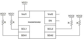
According to my understanding, customers hope that I2C1 and I2C2 can be isolated before powering on. When EN is low level before powering on, the chip is turned off at this time, and the ports are in a high-impedance state, so isolation can be achieved.
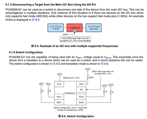
According to your demand analysis, it is similar to the switch configuration mode below.
Question:
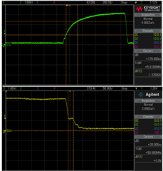
At present, customers have measured that after using PCA9306TDCURQ1, the I2C waveform is not monotonous, as shown below. Is this OK? What is the possible root cause? How to deal with it?