This thread has been locked.

If you have a related question, please click the "Ask a related question" button in the top right corner. The newly created question will be automatically linked to this question.

DS90LV011A: Minimum Output Differential Voltage Conditions?

Part Number: DS90LV011A
Other Parts Discussed in Thread: LMK1D1212

Hi all, 

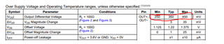
I am investigating the DS90LV011A to be used as a driver for the LMK1D1212 part, which requires a minimum differential input voltage of 300mV.

The DS90LV011A datasheet specs show the following below. My question is under what conditions will the minimum output differential voltage fall to 250mV, and how often this occurs during normal operation of the part?

Thank you.

  • Hi Filipe,

    This device is over 20 years old. We don't have the characterization data for this device anymore.

    This voltage range comes from the LVDS standard, so it's a little strange for the LMK device to require the input differential to be 300mV when the LVDS standard for an input is generally +/-100mV. 

    In general, lower output voltages come from higher temperature due to higher Vth increases and Ron increases at high temps. Other things that can drop an output voltage would be silicon doping which can vary between lots. Lastly a lower supply voltage would generally provide a lower value voltage to a gate of a FET lowering the Ron of the FET resulting in lower output voltage. 

    If the LMK device really does require a 300mV input differential, then it may make sense to use something like an MLVDS driver which generally outputs between 580mV to 650mV which should provide more margin than an LVDS driver.

    Alternatively, we could try to reach out to the team responsible for the LMK device to see if they can tell us if there is more margin on the differential input receiver threshold rather than 300mV.

    -Bobby