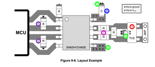
Part Number: SN65HVD485E
Hello, I believe there is an error in figure 9-6 in the datasheet for this part. The figure shows the DE and !RE pins being connected to D and R respectively through resistors, with vias indicating that D and R are directly tied to GND. I believe that the D and R traces should not connect to the pull-down resistors for DE and !RE.
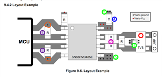
Here is how I believe the figure was intended to look: