This thread has been locked.

If you have a related question, please click the "Ask a related question" button in the top right corner. The newly created question will be automatically linked to this question.

TIC12400-Q1: Need guidance in reading the switch status

Part Number: TIC12400-Q1

Hello Team,

             I have a custom board which has TIC12400-Q1 IC which can be controlled through SPI. I just new to this IC. I tried reading the data from reading the datasheet and trying to read the data from the IC but unable to read the switch status if I short the ground and input line also I can just read '0' please need some guidance in reading the data correctly.

I am able to read the device ID.

But when I try to set the mode to ADC it is not working. I am writing 0xE5FFFFFE to set the mode to ADC state. I just have a doubt can I read the state of the MODE reg. Will it return the state what I set when I was writing?

Please help me reading the states of the switch for channel 12 to channel 17.

What are all the configurations I need to follow to read the ADC status of channel 12 to channel 17?

Please help

  • Hi Vinay,

    I would suggest you read through and try to follow the steps in the Steps to Configure TIC12400-Q1 Multiple Switch Detection Interface (MSDI) application note. (Link)

    Also note that you can only make changes to the configuration registers if the TRIGGER bit in the CONFIG register is set to "0" because once the TRIGGER bit is set to "1" the device locks in the configuration and starts to monitor the inputs.  Therefore, make sure to set TRIGGER to "0" at the beginning of your configuration sequence and then set it to "1" as the final step in your configuration sequence.  This means you will likely make multiple writes to the CONFIG register with different values of the TRIGGER bit.

    It sounds like your difficulties in configuring the registers may be because the TRIGGER bit may be getting set to "1" before you have finished configuring all the registers.

    Regards,

    Jonathan

  • Hello Jonathan,

    I am able to see the switch changes by reading the IN_STAT_COMP reg. But we have a new problem now.

    Initially the INT pin was going low. So I am reading INT_STAT reg before changing the switch states. But when I read INT_STAT reg the INT_PIN is going high. But when I tried to short any line to ground the INT_PIN is not going LOW.

    Is there any change I need to make in the code for changing the INT_PIN states. To make it low there should be a event occurrence. I am giving the event occurrence by making the channel line short to ground. But I can see the SSC(Switch State Change) bit is going high only. it is not getting cleared. 

    Whenever I read INT_STAT reg the SSC bit always stays high. 

    These are all the config I am using in the application.

    THRES_COMP(21h) - set to 2.7v

    INT_EN_COMP1(22h), INT_EN_COMP2(23h) - set to falling edge

    WC_CNF0(1Dh) - set to 2mA wetting current

    I am using COMP mode with continuous setting.

    And I am also using static INT gen.

    I also have one more query.

    We have a active high channel IN0. Which should be connected to VBAT to get the switch State change. Will you please let us know how we can detect the active high channel Switch change event. Configuration to get the output

    Thank you

  • Thank you Jonathan, for the reply.

    Now I am able to read the change of states. But SSC bit always stays high. WIll you please give me the solution.

    Thank you

  • Hi Vinay,

    You will need to set the SSC_EN bit in the INT_EN_CFG0 register (0x24[2] = 1) to enable the INT pin to assert on a Switch State Change (SSC) event.

    You will also then need to configure the INT_EN_CFG1, INT_EN_CFG2, and INT_EN_CFG3 registers to set the specific type of SSC event you want the INT pin to reflect. 

    By default the IN0_EN bits are set to 0x0 which is No Interrupt Generation for IN0.  However, you can set it for a Rising Edge, Falling Edge, or Either a Rising or Falling Edge relative to the Threshold by setting a value of 0x1, 0x2, or 0x3 respectively.

    I assume you simply need to configure these registers and then you will be able to see the INT pin reflect your switch change.

    Regards,

    Jonathan

  • Hello Jonathan,

    INT_EN_CFG1, INT_EN_CFG2, INT_EN_CFG3 are for ADC mode right? Not for Comparator mode. For comparator mode we have INT_EN_COMP1, INT_EN_COMP2 reg's. 

    Thank you

  • Hello Vinay,

    Yes, you are correct.  There are separate registers for the ADC and Comparator interrupt configuration.  I apologize for not including that in my previous response.

    Regards,

    Jonathan

  • Hello Jonathan,

    Will you please guide me how to configure the active high input channels. We have a channel IN_0 which is active high (Short to VBAT). We are unable to configure the active high channel. Will you please let me know the steps to be followed. To read the active high channels.

    Thank you

  • Hello Jonathan,

    We observed there was no INT generated and SSC bit can be observed when we short the channels to GND. We are abled to read whether it is going low using IN_STAT_COMP reg. But INT_PIN is not even changing when channel State got changed. We are out of idea's. We followed all the steps as you mentioned in the document. Still unable to control the INT_PIN. It always stays HIGH. And SSC bit never changed in INT_STAT register.

    We followed this also scpa056.pdf (ti.com)

    And the trigger enabling and disabling you have mentioned it right, that we already implemented.

    Thank you

  • Hi Vinay,

    If you can provide me the final register value for all of the device registers, I can try to replicate your test setup and hopefully identify the issue and offer suggestions.

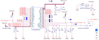
    Given that this is a custom board and not a TI EVM, is it possible to share the portion of the schematic related to the TIC12400-Q1 device?  If so I can review that as well.

    Regards,

    Jonathan

  • Hi Vinay,

    Will you please guide me how to configure the active high input channels. We have a channel IN_0 which is active high (Short to VBAT). We are unable to configure the active high channel. Will you please let me know the steps to be followed. To read the active high channels.

    The configuration is generally the same as for active low inputs.  You will need to enable the channel in the IN_EN register (0x1B) and then select the Current Sink (CSI) setting for that channel in the CS_SEL register (0x1C).  All the other configuration settings such as the wetting current and thresholds remain the same.

    Regards,

    Jonathan

  • Hi Jonathan,

    Sure I have attached the Schematics with this response.  Active High ChannelActive low channel

    Thank you

  • Hi Jonathan,

    Yes I have configured the Active High Channel as per your guidance. But when I give 12V to that channel. We cannot see the state change in the reading. Please help me with the configurations.

    Thank you

  • Hi Vinay,

    The schematics for the switch circuits do not look like they are for the Active High channels which must be connected to one of the IN0 to IN9 inputs.  Can you provide the schematic for the active high inputs and in particular IN0 which you have said you are having difficulty with?

    Can you also look at the voltage on the Input pins with a scope to verify the voltage at the INx pin is crossing the detection threshold?

    Regards,

    Jonathan

  • Hello Jonathan,

    Thank you for the reply. Sure I will share the active high channel schematic with below response. We are using only one Active High channel IN0(Short to VBAT). We are able to see the voltage near the IN0 channel if we give 12V to the channel. But the switch state isnt changing at all. And INT PIN also not responding to Active High input Voltage variations. I set Wetting current as 0mA. And Threshold as 4V. But initially it will be 2.650V but after giving 12V I can see 11.50V in Active High Channel input. But no state change is observed.

    Thank you

  • Hello Vinay,

    Please try setting the wetting current to a higher value.  Setting the wetting current to 0mA effectively disables the current sink and no current will flow through the switch to GND.  This will prevent any voltage difference between an open and closed switch state.

    There is a small amount of leakage current through the MUX specified with a min/max level of +/- 110 uA.  In the 0mA case when there is not an external path for this current to flow, this can hold the INx pin near the VS supply voltage (i.e. 11.5V).  When the current source or sink circuits are enabled, this small leakage current becomes negligible.

    Regards,

    Jonathan