This thread has been locked.

If you have a related question, please click the "Ask a related question" button in the top right corner. The newly created question will be automatically linked to this question.

DS90UB960-Q1: DS90UB960-Q1: Suggested PCB Stackup

Part Number: DS90UB960-Q1
Other Parts Discussed in Thread: DS90UB953-Q1, ,

Good afternoon,

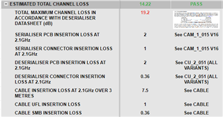
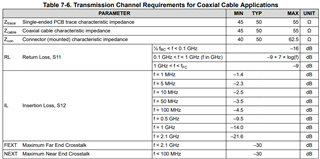
We're trialing a few PCB stack-ups for the best signal integrity to 4 x DS90UB953-Q1 devices (using RG-178 coaxial cable at 3 metre lengths) and appear to be struggling to identify which topology would be best suited to our application.

Could you recommend a suitable PCB stack-up for a design utilising 4 x SMB connectors please operating in synchronous mode at full data throughput (2.1Gbps, ~4.5GHz)?

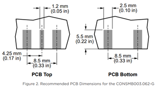
We've trialed 2-layer and 4-layer PCBs with varying results. Our best design was a 2-layer PTFE design with a ZYF255DA core (DK = 2.55, Df = 0.0018) however, we would ideally like to move to (at least) a 4-layer design with an appropriate topology.

All signals on the current design are coplanar waveguide.

Many thanks,

Connor

  • Hello Connor,

    A 4-layer PCB is achievable if your design is simple enough, but we typically recommend a 6-layer PCB, in order  to provide enough GND layers to separate the high-speed signals from the power planes and also to provide a solid GND plane below each high-speed signal for a short return path. In addition, anti-pads are recommended in order to minimize impedance mismatch from component landing pads touching the high-speed DOUT+/- traces.

    A 6-layer PCB is easier to achieve our layout guidelines, but a 4-layer PCB may require much more careful routing.

    For the dielectric material, we recommend a material that is in a similar grade to FR408HR and I-Speed. You can choose material with lower loss characteristics, but that may cost more.

    Best,

    Justin Phan

  • In addition, please aim to meet out Total Channel Requirements across the entire channel (PCB-Cable-PCB). Full details are in the deserializer datasheet, such as the DS90UB960-Q1 datasheet.

  • Hi Justin,

    Thanks for your reply.

    So for a 6-layer PCB design, would you recommend the following topology:

    Signal (with Ground pour)

    Ground

    Signal (or Power with surrounding Ground pour)

    Ground

    Signal (with Ground pour)

    Ground

    Or would it just make more sense to move to an 8-layer design with the following topology:

    Signal (with Ground pour)

    Ground

    Ground

    Power (no Ground pour)

    Signal (with Ground pour)

    Ground

    Signal (with Ground pour)

    I understand the 6-layer board is more difficult from a routing perspective but from a EMI perspective this should be quite good.

    Noted about the dielectric material, thank you. Dk should be around 3.6 (or below).

    Regarding anti-pads, could you clarify whether they need to be on all layers underneath the component landing pads touching the high speed traces? This is something that is difficult to find an answer on. On your DS90UB960-Q1EVM design, there are anti-pads underneath all the ferrite beads touching the high speed traces but they are on multiple ground layers, not just the ground layer directly underneath the high speed signal layer.

    To clarify, I know I need to put anti-pads on the GND plane underneath the high speed signal layer underneath all high speed components (ferrite beads, capacitors, etc.) but "how many layers underneath" the high speed plane is this rule true? All the way through the board? What about a power plane?

  • Hello Connor,

    This really depends on the complexity of your design. As long as you can route all high-speed signals over a continuous GND reference plane, all high-speed signals are spaced away from all neighboring signals and power rails (S>3W), and proper length-matching is achievable, then a 6 layer PCB is possible.

    Your 6-layer PCB sounds okay, but I am not sure of your design requirements or if you can fit everything in 6 layers. The PCB stackup just needs to be symmetrical, which means that each layer above/below the core would need to have the same height. However, this does not strictly define the functionality of each layer. You don't have to strictly only route Power on 1 layer and GND planes on the layer above/below it. But if there are a lot of high-speed signals or the dimensions of your PCB are restricted, then you may have to add layers to allow for more isolation and prevent crosstalk/coupling.

    The 8-Layer stack-up seems a bit redundant, with multiple GND layers on top of each other. One example of an 8-Layer stack-up is:

    SIG - GND - SIG - GND/PWR - GND/PWR - SIG - GND - SIG

    L1 -> L8

    High-speed signals routed on L1, L3, L6, and L8 must be routed over a continuous GND plane. Power planes are also routed on L4 and L5, but they are not routed on top of each other. No high-speed signals are routed over a PWR plane.

    For anti-pads:

    If you route a high-speed signal, then it must always be routed over a continuous GND plane. The trace must also be strictly impedance controlled (e.g. 50-Ohms (+/-10%) single-ended or 100-Ohms (+/-10%) differential). Impedance of a trace consists of multiple factors, such as trace width, distance from the trace to the surrounding GND copper pour, the height of the PCB layer, dielectric material used, etc... If you are on the Top Layer and have a component landing pad touching the high-speed trace, then the landing pad will increase the width of the PCB trace and introduce impedance mismatch. To minimize impedance mismatch, we recommend increasing the distance between the PCB trace and its GND reference plane, to push the impedance of the trace back within the 50 or 100 Ohms tolerance.

    If normally, the high-speed trace is on L1 and you have a GND reference plane on L2, then at the landing pad, you can cut-out the GND plane on L2 just around the landing pads of the capacitors touching the high-speed trace. This will leave an empty space on L2, so the trace on L1 can reference the GND plane on L3 or below.

    If the touching landing pad is relatively small (0402 or 0201), then adding an anti-pad through 1 layer is normally enough. But if the touching landing pad is much larger (0603 or more), then there is typically sharper impedance mismatch and cutting multiple layers may be required. Impedance really depends on the specific stack-up. You can use a calculator tool, such as Saturn, or you can reach out to your fab house to get a recommendation on achieving impedance control. But running a simulation on the trace or using a TDR on the built board is better for confirmation.

    Best,

    Justin Phan

  • Hi Justin,

    Would it be possible to send our latest design to you for review please? I'd like to get your insights as to whether we've produced a suitable design for maximum data throughput.

    Best regards,

    Connor

  • Hello Connor, 

    I can review the PCB stack-up based on any additional material you can share with me. It would also be helpful if you can provide any specific concerns that you are worried about. Just keep in mind that the main requirement that TI has for your system design is if it can meet our defined Total Channel Requirements.

    The DS90UB960-Q1 datasheet has a Channel Requirements section for the max allowable Insertion Loss and Return Loss across the entire FPD3 system (SER PCB -> Cable -> DES PCB). Layout will heavily affect the IL/RL across the high-speed channel. I can offer advice, but customer will need to perform the final verification or simulations.

    Best,

    Justin Phan

  • Hi Justin,

    The stackup is a FR408HR design with a DK of 3.7. I'm using a 6-layer design as follows:

    My areas for concern are as follows:

    1. I have SMB connectors on the edge of the design. I can't get any information from the supplier that tells me how I should route to this connector to make sure 50R impedance is maintained. The connector is a CONSMB003.062-G, 50R impedance, rated to 6GHz with a insertion loss of 0.36dB at 2.4GHz (close to 2.1GHz). The concern here is "What is best practice for this connector to maintain 50R impedance?". Should I put a keepout on L2 under the pad of this connector (except for the trace itself) to ensure the trace width is maintained as close to 50R as possible?

    2. I can't accurately take all the channel requirement parameters as listed in the datasheet however, I've done my best at estimating the total channel requirements from datasheets (which I appreciate isn't the best way of doing this and needs verifying with a VNA when these PCBs arrive). Again, the "concern" here is will the proposed stackup shown give us "the best chance" at getting a low return loss?

    Thanks again for your help.

    Kind regards,

    Connor

  • Hello Connor,

    It seems you are using an RG-178 flexible coaxial cable and an SMB connector in your design. If this is a test board, then that's fine. But typically, customers use automotive grade connectors for improved mechanical strength and reduce EMI/EMC.

    For this specific type of surface-mount SMB connector, I believe the default footprint listed in the datasheet is fine. The only issue I would see is if excess solder is added to the data pin.

    For impedance, if your PCB layer thickness is optimized such that the width of the PCB trace is the same width as the data pin landing pad of the SMB connector while achieving 50-Ohms impedance, then you don't need to add an anti-pad. If the SMB connector SMB landing pad is thicker than the PCB trace coming into it, then you may have to evaluate if it is necessary to add an anti-pad, using a calculator tool like Saturn. Depending on the calculation, you can choose to add or not add an anti-pad depending on which option better maintains 50-Ohms impedance through the connector.

    For the Channel Requirements, the Total Channel Requirements are defined here:

    There is no specific requirement for the IL/RL across the PCB traces or cable. As long as you meet the Total Channel Requirements across two PCBs and a cable (under high temperature and current load conditions), then our SER/DES devices will work as intended.

    The PCB stackup is only a means to meet our Layout Guidelines. As long as you have a stack-up that allows you to route the high-speed FPD-Link traces over a continuous GND plane, maintain 50-Ohms (+/-10%) single-ended impedance all the way from the SER device to the DES device, don't route any noisy signals near the high-speed signal (S>3W), and try to keep the PCB traces as short as possible (to minimize Insertion Loss), choose a cable with decent loss characteristics, choose a dielectric material with decent loss characteristics, then you have the best chance of meeting our Total Channel Requirements.

    If you can't route your high-speed traces to follow these guidelines with your current stack-up, then you may need to add more layers or increase the dimensions of your board.

    IL/RL on the high-speed line also heavily depends on the layout. After performing layout, the only way to get more confirmation on the IL/RL characteristics is to either run a simulation with a software tool like ANSYS, or take physical measurements.

    Best,
    Justin Phan