Part Number: DS250DF230
Hi,
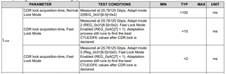
1) How long does it take to reset with the READ_EN_N pin? Please tell me the time required for t1 in the figure below.

2)How long does it take to reset with Address 0x0A? According to the Programming Guide, the CDR Reset is expected to be complete after one access time of the SM Bus. Is this correct?
(Time from when the Reset signal is asserted to when the Reset completes)
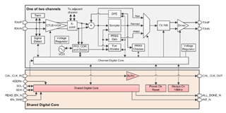
3) I understand that the HW reset in (1) initializes register settings and all circuits in the device, and the SW reset in (2) initializes only circuits related to CDRs. Where in the internal block diagram are the circuits that are not initialized by the SW reset but are initialized by the HW reset?
Best Regards,
Nishie