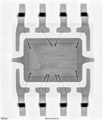
We made X-RAY test and it showed that the ICs voids in the mounting connection of the semiconductor element crystal extend along the entire length and width and occupy more than 10%.
How many percent of voids in the mounting connection is normal?
This thread has been locked.
If you have a related question, please click the "Ask a related question" button in the top right corner. The newly created question will be automatically linked to this question.
We made X-RAY test and it showed that the ICs voids in the mounting connection of the semiconductor element crystal extend along the entire length and width and occupy more than 10%.
How many percent of voids in the mounting connection is normal?
Wade,
This is how all mount and bond devices are assembled: the bond wire attaches the lead frame to the die. The diameter and material of the bond wire are carefully chosen to not add extra parasitic parameters (inductance and capacitance) to adversely affect the performance of the IC. Further, once the device is assembled, it undergoes rigorous testing against the specified limits to make sure it adheres to said specification.
All of that to say this is normal, and there isn't a defined amount of void percentage, it's more about the length, material, and diameter of the bond wires, and the mold compound used. All of this is considered while assembling these devices to assure they perform as defined by the device's datasheet.
Please let us know if you have any other questions.
Regards,
Eric Hackett