Part Number: DS90UB941AS-Q1
Other Parts Discussed in Thread: ALP, USB2ANY
Hello TI team,
Why did 941 register reset itself?
We encounter occasional flickering/black screen phenomenon, and the software detects that the 924_LOCK is link down;
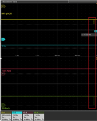
Verify Item:
1.941 1.1V ,1.8V ,PDB are stable, and No I2C Write when 941 register reset;
2.941 patten mode also flicker/black;
HW plateform: QC8155+941+924,DSI as a clock source,Port 1 connect to CID, Port 0 floating
What: screen flicker/black;
Why: 941 register Reset-->941_PIN20 power off--->FPDLINK disconnect(Port1)------>924_LOCK link down---->screen flicker/black
Who: CID display
When: Product normal running, random;
Where: Vehicle