Part Number: PCA9306
Hi,
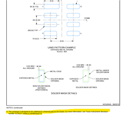
Confused with the PCA9306DQER layout/Footprint of this part.

Didn't understand this note. How to implement this if the selected package do not have a thermal pad.
This thread has been locked.
If you have a related question, please click the "Ask a related question" button in the top right corner. The newly created question will be automatically linked to this question.
Part Number: PCA9306
Hi,
Confused with the PCA9306DQER layout/Footprint of this part.

Didn't understand this note. How to implement this if the selected package do not have a thermal pad.
Hi Sobin,
I believe this is referring to the GND pin on the PCA9306. Datasheet recommends connecting this device to a thermal pad i.e. make the pad on the PCB large enough to cover the entire span of pin 1. Pin 1 should not be connected to a simple trace, but should have some fill/polygon pour that covers the entirety of pin 1 for add thermal dissipation from device to PCB.
Reference section 3.4 of SLUA271.
Regards,
Tyler