This thread has been locked.

If you have a related question, please click the "Ask a related question" button in the top right corner. The newly created question will be automatically linked to this question.

TLIN1021A-Q1: Questions

Part Number: TLIN1021A-Q1

Hi Expert, 

We have some questions related to LIN. Please help check. 

1. The following figure is the internal block diagram of TLIN1021. As shown in the red box, the pull-up resistor used by TLIN1021 is 45KΩ. The pull-up resistor typ value of the slave end specified in the LIN protocol is 30KΩ. What is the reason why the typ value is set larger than that of the LIN protocol? We believe that larger pull-up resistors will affect the driving ability of the LIN bus and have an impact on the signal under multiple loads.
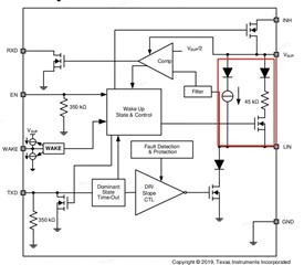
2. Related to the above question, what is the function of the current source on the left side of the pull-up resistor in the red box?

3. The LIN protocol stipulates that the length of the LIN bus shall not exceed 40m. How is this bus length calculated? Does it include the length of the bus and each node branch?

4. How to understand the four specified Duty cycles? Are these different duty cycle related to different working voltages? Are these required to be covered during testing? When performing hardware testing, what timing indicators must be tested and verified?

Thanks!

Ethan Wen

  • Hi Ethan,

    We've assigned one of our subject matter experts to this thread. They should get back to you soon.

    -Bobby

  • Hi Ethan,

    1. 30KΩ is just the typ value, right? There is also min 20KΩ and max 60KΩ by LIN standard. The LIN standard recommend a typ 30KΩ ≠ Our device must integrate exactly 30KΩ typ. TLIN1021A's internal pullup is still within the range of 20-60KΩ. The pullup resistors at the slaves just to ensure a valid voltage level if the connection to the master is broken. I don't think 45KΩ would be a problem.

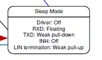
    2. It's a weak current pull-up which is active in Sleep mode to prevent false wake-up events in case an external connection to the LIN bus is lost.

    3. This definition allows for the designer to design without too much worry regarding the capacitance and inductance of the cable. Please take a look of 4.3 in TI's LIN physical layer requirements:

    https://www.ti.com/lit/an/slla383a/slla383a.pdf?ts=1711060394287&ref_url=https%253A%252F%252Fwww.google.com%252F

    In reality, you can violate this 40m specification while LIN still works. If you are using some really small capacitance cable I would expect the capability to transmit at 80m. But if someone ask me why LIN fails at 41m, I'll just tell him because he violates the specification. 

    4. See 3.6 in LIN physical layer requirements above. 

    From ISO17987, receiver propagation delay time and symmetry of receiver propagation delay time need to be verified.

    Regards,

    Sean